


MXN2512概述:
MXN2512是VDS=20V,ID =10A,@VGS=4.5V,RDS(ON)(Typ.)=7.2m?,@VGS=4.2V,RDS(ON)(Typ.)=7.4m?,@VGS=3.8V,RDS(ON)(Typ.)=8m?,@VGS=2.5V,RDS(ON)(Typ.)=10m?的Dual N-Channel MOSFET.MXN2512提供DFN5x2-6L封装.
The MXN2512 uses advanced trench technology to provideexcellent RDS(ON), low gate charge and operation with gate voltages as low as 2.5V. This device is suitable for use as aload switch or in PWM applications.it is ESD protected.
MXN2512特性:
VDS =20V,ID =10A
@VGS=4.5V RDS(ON)(Typ.)=7.2m?
@VGS=4.2V RDS(ON)(Typ.)=7.4m?
@VGS=3.8V RDS(ON)(Typ.)=8m?
@VGS=2.5V RDS(ON)(Typ.)=10m?
ESD Rating: 2000V HBM
Asvanced trench MOSFET process technology
Ultra low on-resistance with low gate charge
New Thermally Enhanced DFN5X2-6L Package
MXN2512应用:
PWM applications
Load switch
Battery charge in cellular handset
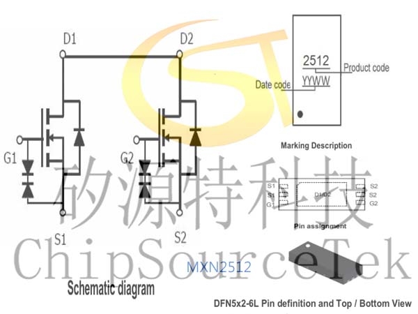
MXN2512典型应用及引脚图:

服务热线:
13823761625


 发送邮件
发送邮件 商务QQ客服
 13823761625

