


The United States is attacking the "mother of chips"! How does EDA software affect the entire semiconductor industry?
Time:2022-08-19
Views:1748
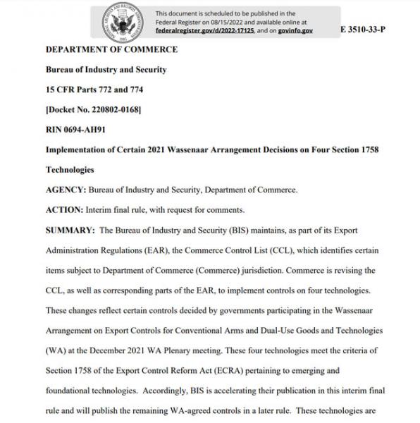
According to the associated press, the US Department of Commerce on Friday issued a provisional final regulation on the ECAD software necessary for the design of gaafet (full gate field effect transistor) structure integrated circuits; Ultra wide band gap semiconductor materials represented by diamond and gallium oxide; New export controls will be implemented on four technologies such as pressure gain combustion (PGC) used by gas turbine engines.
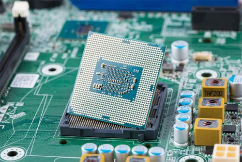
It is reported that gaafet transistor technology is more advanced than FinFET transistor technology. FinFET technology can achieve 3nm at most, while gaafet can achieve 2nm. Gallium oxide (Ga2O3) and diamond are the fourth generation semiconductor materials that are widely concerned.
What is the impact of EDA software restrictions? As strong as Samsung, the manufacturing technology of 3nm GAA architecture just broke through in June was also completed with the full assistance of EDA software such as ANSYS, Synopsys and cadence. Without the cooperation of EDA software, it is more difficult to break through the limitations of architecture and process.
The United States has implemented new export controls on four technologies including EDA tools
According to the financial Associated Press, on Friday, local time, the industry and Security Bureau (BIS) of the US Department of Commerce disclosed in the federal Gazette a provisional and final decision to increase export restrictions, involving advanced semiconductor, turbine engine and other fields.
According to the communique, the U.S. industry and security administration decided to amend the Department of Commerce control list (CCL) and the export administration regulations (ear) simultaneously to control the four technologies.
Alan Estevez, deputy secretary in charge of industry and security of the US Department of Commerce, introduced that the scientific and technological progress that enables technologies such as semiconductors and engines to operate faster, more efficiently and for a longer time, as well as under worse conditions, may "change the rules of the game" in the commercial and military environment.
It is reported that the technologies upgraded for export control include:
Wide band gap semiconductor materials gallium oxide (Ga2O3) and Diamond: gallium nitride and silicon carbide are the main materials for producing complex microwave and millimeter wave equipment or high-power semiconductor devices. Gallium oxide and diamond have the potential to manufacture more complex equipment and can withstand higher voltage or temperature.
Develop EDA software for gaafet (full gate field effect transistor) structure integrated circuit: electronic computer aided software (EDA / ECAD), which is used to design, analyze, optimize and verify the performance of integrated circuit or printed circuit board. As the successor of FinFET, gaafet (full gate field effect transistor) is considered as the key technology of mass production process of 3nm and below. BIS is also soliciting public opinions to determine which specific functions of ECAD are particularly suitable for designing gaafet circuits to ensure that the US government can effectively implement this control.
Pressure gain combustion technology (PGC): this technology has the potential to improve the efficiency of gas turbine engines by more than 10%, potentially affecting aerospace, rockets and hypersonic missile systems. PGC technology uses a variety of physical phenomena, including resonance pulse combustion, constant volume combustion and detonation, resulting in an increase in the effective pressure across the burner, while consuming the same amount of combustion. BIS is unable to confirm that any engine in production uses this technology at present, but there are a lot of studies pointing to potential production.
How important is EDA, the "mother of chips"?
According to Tianfeng International Research Report, EDA, electronic design automation, is known as the "mother of chips".
If chip manufacturing is compared to building a building, IC design is the design drawing of the building, and EDA software is the design tool of this drawing. However, the complexity of EDA software is N orders of magnitude higher than that of architectural design software.
Using EDA tools, electronic designers can design electronic systems from concepts, algorithms, protocols, etc., and can automatically process the entire process of electronic products from circuit design, performance analysis to designing IC layout or PCB layout on the computer. And is one of the strategic foundation pillars throughout the entire integrated circuit industry chain. EDA technology can be widely used in electronics, communications, aerospace, machinery and other fields.
Therefore, in general, EDA is a "small and fine" link in the field of integrated circuit industry, with small output value but extremely important. According to the data of CCID think tank, the global EDA market scale increased from US $6.22 billion to US $7.23 billion in 2018-2020, with an annual compound growth rate of 7.81%. Compared with the hundreds of billions of dollars of integrated circuit industry, it is not worth mentioning, but without this product, all chip design companies in the world will have to shut down.
The first echelon: at present, the EDA industry has a high market concentration and is monopolized by nearly 80% of the three international EDA Giants: Synopsys, cadence and mentor graphics (acquired by Siemens in 2016).
The three EDA giants hold the absolute dominant power, and their products have a market share of 85% in China. They have their own characteristics in products, and their IP priorities and advantages are quite different. Therefore, many first-line chip design manufacturers have used different EDA IPS of two or three of them to design chips at the same time.
The second echelon: enterprises represented by ANSYS, SILVACO, aldec Inc and Huada Jiutian. This type of enterprise has the whole process of specific fields and is leading in technology in some fields.
The third echelon: enterprises represented by Altium, concept engineering, introduction electronics, guangliwei, silcore, downstream technologies, etc. The layout of such enterprises in EDA is mainly based on point tools, lacking full process products in specific areas of EDA.
EDA localization has a long way to go
According to open source Securities Research Report, benefiting from the support of integrated circuit localization policy, EDA localization rate increased from 6.24% in 2018 to 11.48% in 2020.
According to China electronic news, recently, two EDA companies, Huada Jiutian and gailun electronics, landed in the A-share market and achieved excellent performance of the first day of the big rise. This is a clear contrast with the situation in which some semiconductor companies were listed and broke, showing that the capital market is optimistic about the EDA industry. With the support of new technologies and applications such as artificial intelligence and 3D packaging, the new growth space of EDA industry is being opened.
On July 29, Huada Jiutian, a domestic EDA leader, officially landed on the gem, with an increase of 126% on the first day of listing. The market value exceeded 40 billion yuan at one stroke, and the issuance P / E ratio of 333 times also broke the historical record of the gem. Guangliwei landed on the gem on August 5, and the closing price was 156% higher than the issuing price. On the same day, Galen electronics rose by 12.86%.
EDA‘s stock market shows resilience against the trend. West China Securities research report pointed out that EDA tools are necessary tools for integrated circuit design, manufacturing, packaging, testing and other work, and need to be constantly updated. The industry‘s awareness of the urgency and necessity of the development of China‘s EDA industry has significantly improved.
However, a new problem, that is, the small and scattered domestic EDA industry, has also emerged.
In the previous interview, Lin KaiPeng, senior vice president of Guowei Sili, pointed out that at present, the domestic EDA industry is in the early competitive stage of industry development. Some enterprises may have certain advantages in individual tools or some subdivisions, but the short board is not comprehensive enough, and no one can cover the entire EDA industry chain. It is difficult to provide full process products, which is the main problem of domestic EDA enterprises.
In view of such a situation, Yang Ye, director of product and business planning of core Huazhang technology, believes that "in the early stage of development, domestic industry should pay more attention to advocating ‘openness‘ and strengthen the cooperation among enterprises. The purpose is to strengthen the synergy among tools, build a more perfect industry ecology and improve the efficiency of chip verification. Domestic EDA enterprises should not be greedy for perfection in the initial stage, but should concentrate on doing what they are best at and jointly build an open and prosperous ecosystem."
|
Disclaimer: This article is transferred from other platforms and does not represent the views and positions of this site. If there is infringement or objection, please contact us to del |


 Business consulting

 13823761625
 Mail me