


How do you view Huawei has completed the localization of EDA tools with chips above 14nm
Time:2023-03-28
Views:1010
At the hardware and software tool oath conference held recently by Huawei to "break through the Wujiang natural danger and achieve strategic breakthrough", Huawei‘s rotating chairman Xu Zhijun stated that Huawei‘s chip design EDA tool team, in conjunction with domestic EDA companies, has jointly created EDA tools required for processes above 14 nm, basically achieving the localization of EDA tools above 14 nm, and will complete its comprehensive verification in 2023.
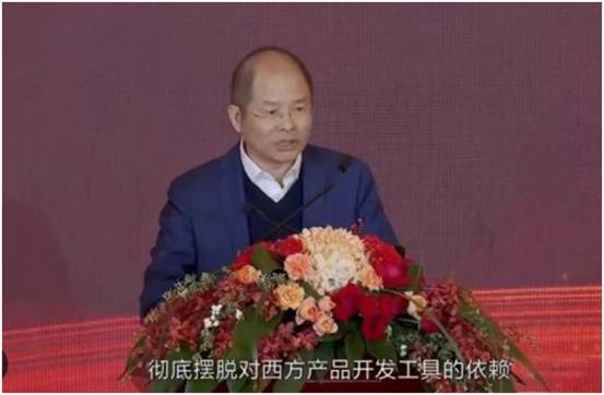
In his speech, Xu Zhijun pointed out that over the past three years, Huawei has completed the replacement of 78 software/hardware development tools around three R&D production lines: hardware development, software development, and chip development, ensuring the continuity of R&D operations.
The software development tool development team has been laying out since 2018, striving to create a complete tool chain for software from coding, compilation, testing, security, construction, release, and deployment. The strategy of self research and joint development with partners is adopted to solve the problem of tool continuity; With the support and assistance of partners, the hardware development tool development team has broken through the root technology, introduced new architectures, released cloud native schematic tools, created high-speed and high-density PCB layout tools, polished structural design 2D/3D CAD tools, and laid out hardware multidisciplinary simulation tools; Huawei has also worked with its partners to lay out EDA chip design tools, expand its independent choice of EDA tool software, seize the opportunity in the chip design market, and basically achieve the localization of EDA tools above 14 nm. In 2023, it will complete its comprehensive verification.
"As of today, our joint partners have released 11 product development tools to the outside world, and all product lines have been switched to our own released tools. Partners and customers can also use them on Huawei Cloud. Currently, there are approximately 200000 software developers and 197000 hardware developers using the tools we developed or jointly developed with our partners every month, and 203 enterprises are willing to pay for using us." "Is a recognition of the development tool team." Xu Zhijun said.
Recently, Huawei founder Ren Zhengfei stated that in three years, Huawei has completed the replacement development of over 13000 devices and the repeated replacement development of over 4000 circuit boards. Although Huawei is still in a difficult period, it has not stopped on the way forward. In 2022, Huawei‘s research and development expenses reached 23.8 billion US dollars. In a few years, as the company‘s profits increase, it will continue to increase investment in cutting-edge exploration.
Xu Zhijun also said, "Although we have achieved many breakthroughs in product development tools over the years, there are still many challenges ahead, and there are also many product development tools that have not been completely breakthrough. We need to keep on working and redouble our efforts to continuously attract global talents and thoroughly achieve strategic breakthroughs."
How do you think of "Huawei has completed the localization of EDA tools with chips above 14nm"? After communicating with industry insiders, the author reached the following conclusions:
1. EDA tools are divided into front-end and back-end. According to Huawei, this should be the completion of the localization of back-end tools, which is also a major breakthrough! Congratulations!
2. Currently, EDA tool manufacturers in China are striving to achieve full process tools. Only by achieving full process tools can we completely overcome the bottleneck situation. Based on the results of the author‘s communication with EDA manufacturers in the industry at several conferences last year, there will be significant breakthroughs in local EDA in the next two years, and everyone can elaborate.
3. EDA tools are basically based on SPICE device models combined with their own algorithms for circuit simulation. The key to the basic models being consistent is that they implement different methods, just as everyone knows how shoes are made, but the methods used can vary. Currently, artificial intelligence technology and big data applications have brought new variables to the EDA field, and the world‘s top EDA manufacturers are basically derived from Chinese Daniel, Therefore, it will be a matter of time before local EDA breakthroughs in this field. What local manufacturers lack is the collaborative verification of talent and upstream and downstream links.
4. With the change of China‘s innovation system, there will be major breakthroughs not only in the EDA field, but also in the IC manufacturing and packaging testing fields in the future.
|
Disclaimer: This article is transferred from other platforms and does not represent the views and positions of this site. If there is any infringement or objection, please contact us to delete it. thank you! |


 Business consulting

 13823761625
 Mail me