


Domestic EDA verification and debugging tools achieve breakthroughs, helping to improve chip design efficiency
Time:2023-11-27
Views:463
After decades of development, every aspect of chip design now cannot be separated from the participation of EDA tools, involving the entire process of verification, debugging, logic synthesis, layout and wiring. Especially in the critical verification and debugging stages, it can be said that it is the "dual pulse" of chip fabrication. If obstructed in this stage, the "secondary damage" it will bring will be unimaginable.

Especially in the current situation where the market share of domestic EDA tools is mostly occupied by foreign giants, on the one hand, the United States continues to increase its constraints, and the "bottleneck" intensity is becoming increasingly severe; On the other hand, most international giant tools are increasingly tending towards closed processes. With the booming development of the domestic semiconductor industry, how domestic EDA manufacturers focus on solving the problem of tool from 0 to 1 has become a new mission of the times.
Seizing this opportunity, Shanghai Hejian Industrial Software Group Co., Ltd. (hereinafter referred to as "Hejian Software"), which has established a multi-point layout in the field of EDA tools, has recently launched a new UVD debugging tool to help domestic semiconductor design manufacturers pass the verification and debugging stages.
Verification and debugging require collaborative operations
The reason why verification and debugging are crucial is closely related to the design requirements of digital chips and the product iteration of design companies.
At present, the scale of digital chips often exceeds billions of gates, and with the advancement of technology, the cost of chip fabrication remains high, and the loss of chip failure is difficult to estimate. More importantly, redesigning not only means a huge investment in research and development costs, but also leads to missing the time window for product launch and the opportunity for growth and development. This is an unbearable burden for any design company.
Many aspects of the chip process from design to production cannot be separated from verification and debugging. Verification is to ensure that the design meets functional and performance requirements, while debugging is to identify defects discovered during the verification process, identify the true cause of the problem as soon as possible for repair. Therefore, verification and debugging become the key links to unlocking the success or failure of the chip.
"With the increasing complexity and integration of SoC chips and the expansion of the scale, the proportion of verification work is getting higher and higher, which can reach more than 70%. In general, the basic configuration in the design team is that a design engineer should be equipped with 2-3 verification engineers. Among them, the workload of debugging can account for more than 40% of the verification work." Gao Bo, the senior research and development director of UIS, digitally describes the "responsibility" of verification and debugging.
Correspondingly, the challenges for validation and debugging tools are increasing day by day.
Gao Bo pointed out that verification tools and debugging tools complement each other, and the mission is to quickly achieve verification convergence. Ensuring coverage, sufficient and early detection of issues is a challenge for validation tools; Debugging tools need to help users analyze and solve functional and performance issues more quickly, while analyzing and debugging coverage related issues can accelerate coverage convergence.
In addition, collaborative "combat" is also a necessary condition. Gao Bo further mentioned that at the verification level, different verification tools such as formal verification and FPGA prototype verification are involved. To meet the verification requirements, it is not only required that the verification tools can work together and cooperate with each other to achieve sufficient verification coverage and achieve verification convergence; At the same time, debugging tools as a platform should be able to support debugging of all validation tools and support debugging under collaborative simulation of different validation tools.
Achieve breakthrough from 0 to 1
It has to be said that international manufacturers have already taken a leading position in the field of EDA verification and debugging tools, but there is still room for competition and opportunities to break through for the emerging domestic EDA manufacturers.
"The architecture and technology of verification and debugging tools need to be constantly innovated with the development of verification processes and methodologies. Foreign manufacturers inevitably have burdens due to long-term accumulation. At the current time point, domestic EDA manufacturers can stand at a higher starting point, design product architecture and functions based on a comprehensive verification panorama, solve problems from 0 to 1, and achieve new breakthroughs." Gao Bo is full of confidence in this.
Obviously, focusing on the requirements of debugging tools and cultivating a stable and efficient verification and debugging platform has become an important task for domestic EDA manufacturers.
Gaobo mentioned that the industry‘s requirements for debugging tools focus on: in terms of performance, ensuring high performance and large capacity; Starting from ease of use, it is necessary to be concise, easy to use, and smooth to ensure the overall efficiency of debugging. In addition, at the system level, it is necessary to fully support collaborative simulation between various verification tools.
In this process, it is even more important to keep up with the times. Gao Bo stated that during the iteration process, validation and debugging tools should continuously introduce innovative validation methodologies and processes, not only supporting functional debugging, but also expanding to debugging in areas such as power consumption, coverage, and security; Not only do we need to support different design levels such as RTL and Gate level requirements, but we also need to support transaction level and system level validation and debugging.
"Only through continuous internal and external training can we continuously improve the efficiency of verification and debugging, accelerate verification convergence." Gao Bo explicitly stated.
For the development path of domestic EDA manufacturers for verification and debugging, Gaobo believes that it is necessary to not only work steadily but also lay out long-term plans.
"After creating a debugging platform that meets the above needs, we should firmly implement the application of the actual projects of domestic semiconductor customers to solve the debugging problems in the projects. We should also embrace the actual needs of local customers with an open mind to achieve differentiated advantages. After the products become available, we can further strengthen cooperation, continue to polish the products, constantly break through the technical burden and technical barriers of existing tools, and further improve Verify and debug efficiency, achieve good usability and durability, and move towards a win-win situation Gao Bo put forward a fair suggestion.
The New Advancements of UVD
Based on profound insights into verification and debugging tools, combined with the accumulated technical resources of the Hejian Software team in the field of digital chip verification, as well as unwavering architectural innovation, Hejian Software has taken the lead and has been continuously investing in debugging tools while focusing on the development of various core verification tools. Now, it has welcomed the launch of UVD.
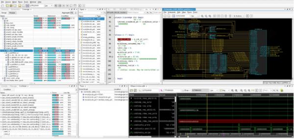
(Image: UVD main interface)
Gaobo explained in detail that the advantages of Hejian Gongsoft UVD are reflected in its simplicity and ease of use, adopting advanced UI technology with a simple interface that adapts to the functions used, greatly improving the user experience. The second is high efficiency and performance, which are reflected in the processing efficiency and interactive performance of large-scale data. For example, high-performance waveforms can compete with mainstream products in the current market, and the compression ratio with VCD (Value Change Dump) can reach tens to thousands of times.
It is worth mentioning that the design of the architecture and data interface of Hejian Software UVD is "long-term": it supports debugging of different validation tools and unified and collaborative debugging of data between different tools.
And this is in line with the multiple EDA products and solutions released by Hejian Software, including digital simulators, FPGA prototype verification systems, advanced packaging collaborative design environments, etc., which have taken the lead in breaking through the difficult fields of digital verification and collaborative design and laid the foundation, complementing each other.
Specifically, Hejian Software UVD provides a unified waveform and coverage data interface, which can be integrated with other validation tools, promoting data integration and collaboration among different validation tools. This is currently not supported by many mainstream tools. In addition, UVD can support integrated debugging of testing environment, design, and coverage based on native architecture. For example, the source code window of UVD has reserved support for IDE, which can be easily extended in the future to help design engineers improve efficiency.
In addition, all products of Hejian Gongsoft are based on innovative design, fully considering the collaboration between different products. For example, UVD can collaborate with the verification testing management platform VPS of Hejian Gongsoft to accelerate the debugging of defects and coverage in regression testing.
"Hejian Gongsoft has already built a relatively complete EDA digital verification solution, and as a debugging tool, UVD has received positive feedback in customer trials. Perhaps the customer‘s agreement is the best evidence of UVD‘s strength.".
Nowadays, with the rapid development of technology by domestic semiconductor design manufacturers, more and more world-class IC design companies have emerged. In this optimistic situation, Hejian Gongsoft deeply realizes that domestic EDA manufacturers will further strengthen the foundation for local manufacturers to look globally through mutual promotion and progress with IC manufacturers.
After continuously achieving a good start, Hejian Gongsoft, which took advantage of the situation, has also set higher goals.
Gao Bo finally stated that Hejian Gongsoft has numerous senior experts in the field of verification, and the technical team is very experienced. Hejian Gongsoft will continue to combine its unique local advantages, maintain an open mindset, embrace an open architecture, and promote the establishment of a good EDA ecosystem. At the same time, it will innovate and continuously polish the architecture in the field of EDA tools for domestic verification and debugging, and assist domestic semiconductor design companies in providing full process services.
|
Disclaimer: This article is transferred from other platforms and does not represent the views and positions of this site. If there is any infringement or objection, please contact us to delete it. thank you! |


 Business consulting

 13823761625
 Mail me