


Analysis of problems in TWS earphone design
Time:2022-04-02
Views:2163
Some common problems that are easy to appear in the design process are summarized today.
1. The two CC1 and CC2 pins of type-C USB in the charging bin cannot be short circuited together, but should be connected to the pull-down resistance independently:
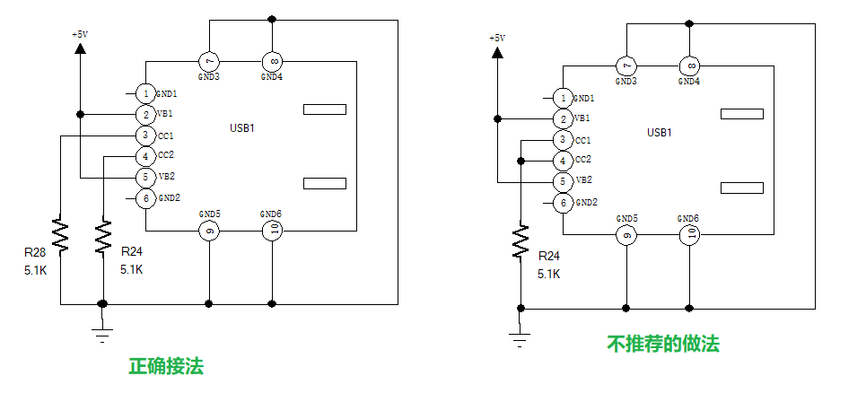
If CC1 and CC2 are short circuited, the PD adapter will fail to charge, because the PD equipment needs to be tested
2. The distance between the hall device on the charging box and the magnet should be controlled within 3mm. If it exceeds this distance, detailed reliability verification needs to be done, because the magnet will demagnetize after high temperature. If the distance between the two is too far, hall induction failure may occur
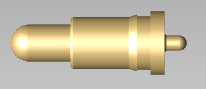
3. PCB through holes shall be made at the bottom of the charging thimble to ensure the reliability of the design
4. MIC of earphone must have sealing design, especially for projects with ANC and enc functions
5. The charging thimble and pad on the headset PCB are recommended to be designed according to the following proportion:
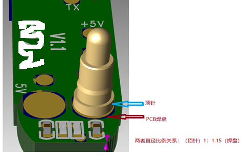
Because if the thimble is larger than the PCB pad, the reliability will not pass, and there may be a risk of falling off during barrel test
6. The speaker of the earphone and the battery should not be too close. They are very easy to interfere with each other, especially some high-sensitivity speakers, which are more likely to be interfered. For example, you can hear noises So be very careful
7. The cable length of the battery should be well controlled, which will have some impact on RF
8. Antenna: the stability of RF signal is the core hard index The antenna types are mainly ceramic antenna and FPC antenna The performance index of the antenna and the placement position of the antenna must be verified before mold opening Once the structure mold is finalized, it is difficult to change The RF performance of PCBA is easy to verify. The most troublesome thing is the coordination between PCBA and structure, and the coordination between antenna and structure is the most time-consuming
|
Disclaimer: This article is transferred from other platforms and does not represent the views and positions of this site. If there is infringement or objection, please contact us to delete. thank you! |


 Business consulting

 13823761625
 Mail me