


Application of DC-DC boost regulator in low power portable system
Time:2022-04-07
Views:2161
The power supply of portable electronic devices (such as smart phones, GPS navigation systems and tablets) can come from low-voltage solar panels, batteries or AC-DC power supply. Battery powered systems usually stack batteries in series to achieve higher voltage, but this technology may not always be feasible due to insufficient space. Switching converters use inductive magnetic fields to store electric energy alternately and release it to the load at different voltages. Because the loss is very low, it is a good and efficient choice. The capacitance connected to the output of the converter can reduce the output voltage ripple. The boost converter discussed in this paper provides higher voltage; The buck converter discussed in the previous article 1 provides a lower output voltage. The switch converter with built-in FET as the switch is called the switch regulator, 2 and the switch converter requiring external FET is called the switch controller. 3
Figure 1 shows a typical low-power system powered by two AA batteries in series. The electrically available output range is about 1.8 V to 3.4 V, while the IC requires 1.8 V and 5.0 V for operation. The step-up converter can increase the voltage without
increasing the number of battery units, so as to power WLED backlight, micro hard disk drive, audio equipment and USB peripherals, while the step-down converter can power, memory and display.

Figure 1 Typical low power portable system
The inductance hinders the tendency of current change and provides a boost function. During charging, the inductor is used as a load and stores electric energy; When discharging, it can be used as power supply. The voltage generated in the discharge process is related to the current change rate and independent of the original charging voltage, so different input and output levels can be provided.
The boost regulator consists of two switches, two capacitors and one inductor, as shown in Figure 2. The non overlapping switch driving mechanism ensures that only one switch is on at any time to avoid bad through current. In stage 1 (ton), switch B opens and switch a closes. The on inductor is connected to ground, so the current flows from VIN to ground. Because the inductor terminal is a positive voltage, the current increases and the electric energy is stored in the inductor. In stage 2 (toff), switch a opens and switch B closes. The inductor is connected to the load, so the current flows from VIN to the load. Since the inductor terminal has a negative voltage, the current decreases and the energy stored in the inductor is released into the load.
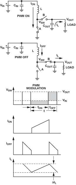
Figure 2 Topology and working waveform of Buck Converter
Note that the switch regulator can work continuously or intermittently in continuous conduction mode (CCM). When working, the inductive current will not drop to 0; In intermittent conduction mode (DCM), the inductance current can be reduced to 0 when working. The current ripple is shown in Figure 2 as Δ IL usage formula Δ IL = (VIN? Ton) / L. calculation. The average inductance current flows into the load and the ripple current flows into the output capacitor.
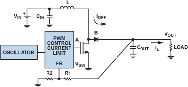
Figure 3 The boost regulator integrates oscillator, PWM control loop and switching FET
The regulator using Schottky diode instead of switch B is defined as asynchronous (or asynchronous), while the regulator using FET as switch B is defined as synchronous. In Fig. 3, switches a and B have been implemented using an internal nFET and an external Schottky diode, respectively, to form an asynchronous boost regulator. For low-power applications that require load isolation and low off current, an external FET can be added, as shown in Figure 4. Drive the EN pin of the device below 0.3 V to turn off the regulator and completely disconnect the input and output.
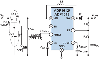
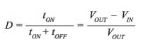
Figure 4 Adp1612 / adp1613 typical application circuit
Modern low-power Synchronous Buck Regulator takes pulse width modulation (PWM) as the main working mode. PWM keeps the frequency unchanged and adjusts the output voltage by changing the pulse width (ton). The average power delivered is proportional to duty D, so it is an effective way to provide power to the load
D=(15-5)/15=0.67 or 67%.
Due to the reduced power consumption, the input power must be equal to the power transmitted to the load minus all losses. Assuming that the conversion is very effective, a small amount of power loss can be omitted from the basic power consumption calculation. Therefore, the input current can be approximately expressed as:
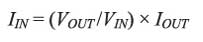
For example, if the load current is 300 Ma at 15 V, iin = 900 Ma at 5 V - three times the output current. Therefore, the available load current decreases as the boost voltage increases.
The boost converter uses voltage or current feedback to adjust the selected output voltage; The control loop can maintain output regulation according to load changes. The operating frequency range of low-power boost converter is generally 600 kHz to 2 MHz.
When the switching frequency is high, the inductance used can be smaller, but each time the switching frequency is doubled, the efficiency will be reduced by about 2%. In adp1612 and adp1613 boost converters (see Appendix), the switching frequency can be selected through pins. The working frequency under very high efficiency is 650 kHz and that of small external devices is 1.3 MHz. For an operating frequency of 650 kHz, connect freq to GND and 1.3 MHz to VIN.
Inductance is the key device of the boost regulator. It stores electric energy during the power switch on, and transmits the electric energy to the output through the output rectifier during the power switch off. In order to achieve a balance between low inductance current ripple and high efficiency, the adp1612 / adp1613 data book recommends an inductance value range of 4.7 μ H to 22 μ H。 In general, lower inductance has higher saturation current and lower series resistance at a given physical size, while lower inductance leads to higher peak current, which can reduce efficiency and increase ripple and noise. It is usually good to perform boost in intermittent conduction mode in order to reduce the inductance size and improve stability. The peak inductance current (large input current plus half of the inductance ripple current) must be less than the rated saturation current of the inductance; The large DC input current of the regulator must be less than the current RMS rating of the inductor.
Main specifications and definitions of Boost Regulator
Input voltage range: the input voltage range of the boost converter determines the low available input power supply. The specification may provide a wide input voltage range, but the input voltage must be lower than Vout to achieve efficient operation.
Ground current or quiescent current: DC bias current (IQ) not transmitted to the load. The lower the IQ, the higher the efficiency. However, IQ can be specified for many conditions, including off, zero load, PFM operating mode or PWM operating mode.
Therefore, in order to determine a good boost regulator for an application, it is good to check the actual working efficiency under specific working voltage and load current.
Turn off current: This is the input current consumed by the device when the enable pin is disabled. Low IQ is very important for whether the battery powered device can stand by for a long time in sleep mode.
Switch duty cycle: the working duty cycle must be less than a large duty cycle, otherwise the output voltage cannot be adjusted.
For example, d = (VOUT – VIN) / Vout When Vin = 5 V and Vout = 15 V, d = 67% Adp1612 and adp1613 have a large duty cycle of 90%.
Switch duty cycle: the working duty cycle must be less than a large duty cycle, otherwise the output voltage cannot be adjusted. For example, d = (VOUT – VIN) / Vout When Vin = 5 V and Vout = 15 V, d = 67% Adp1612 and adp1613 have a large duty cycle of 90%.
Current limiting: boost converters usually specify peak current limits instead of load current. Please note that the greater the difference between VIN and Vout, the lower the available load current. The peak current limit, input voltage, output voltage, switching frequency and inductance value all determine the large available output current.
Line adjustment rate: line adjustment rate refers to the change rate of output voltage with the change of input voltage.
Load regulation rate: load regulation rate refers to the change rate of output voltage with the change of output current.
Soft start: it is very important that the boost converter has a soft start function. The output voltage rises slowly in a controllable way during start-up, so as to avoid output voltage overshoot during start-up. The soft start of some boost converters can be adjusted by external capacitance. As the soft start capacitor charges, it limits the peak current allowed by the device. With the adjustable soft start function, the start time can be changed to meet the system requirements.
Thermal shutdown (TSD): when the node temperature exceeds the specified limit, the thermal shutdown circuit will close the regulator. The always high junction temperature may be caused by high working current, poor cooling or high ambient temperature. The protection circuit includes hysteresis to prevent the device from returning to normal operation after the on-chip temperature drops below the preset limit after thermal shutdown
Undervoltage lockout (UVLO): if the input voltage is lower than the UVLO threshold, the IC will automatically turn off the power switch and enter the low power consumption mode. This prevents possible operating instability at low input voltage and prevents the power supply device from starting when the circuit cannot control it.
Concluding remarks
The low-power boost regulator simplifies the design of DC-DC converter by providing mature meter. The application part of the data manual provides design calculation, and adisimpower4 design tool can simplify the tasks of end users.
|
Disclaimer: This article is transferred from other platforms and does not represent the views and positions of this site. If there is infringement or objection, please contact us to delete. thank you! |


 Business consulting

 13823761625
 Mail me