


Circuit diagram of class a headphone amplifier driven by operational amplifier
Time:2022-04-11
Views:2157
Using the class a amplifier introduced in this paper, a better high fax effect can be obtained. Class a headphone amplifier (tl072op with bc142143)
In daily life, when other family members are watching TV, or others are sleeping and can‘t be disturbed, you can‘t enjoy the beautiful music. In this case, we need to consider the amplifier introduced in this paper. Although the circuit is very simple, its high fax effect exceeds the standard power amplifier in the store. Using the tuner and answering machine movement, we can install a high-quality sound system, but the price is lower.
Design idea: before introducing the circuit in detail, let‘s talk about the design idea and explain how to achieve class a performance, and most experience sound power amplifiers use class B.
As we know, the output stage of a general amplifier consists of two branches: one branch processes the negative (negative half cycle) output signal, and the other branch processes the positive (positive half cycle) output signal. In this way, the static current can be minimized, but to drive the speaker, the voltage and current must have a large amplitude.
Unfortunately, these amplifiers have some distortion, called cross distortion. It appears at or near the zero crossing point of the output signal. If the two branches of the circuit are not completely matched, there will often be cross distortion, which makes the effect of listening to programs with headphones very poor.
Connecting the socket of the earphone to the output of the main amplifier also causes another problem: some resistors need to be connected in series between the earphone and the output stage to reduce the signal level. This will change the original negative feedback characteristics, which usually leads to a peak in the bass response, accompanied by a rapid roll down below the peak frequency.
In short, in order to produce an amplifier that can successfully drive headphones and obtain the best sound quality, the above two problems need to be solved.
To successfully design any kind of audio equipment, the first step is to find out what equipment is designed and determine its circuit. Ten years ago, the impedance of most earphones was 8 Ω, but now most of them use polyester diaphragm diaphragm, and the impedance is usually 32 Ω.
If you go to several high fax stores, you will find that the sensitivity of most products (including those with impedance of 8 Ω) is 87db-96db / MW, and the maximum input power is nearly 100MW. Through the test after installing this amplifier on 10 pairs of headphones, it is found that most headphones can output enough volume with input power of 10MW.
Class a power amplifier: for output power, the amplifier also needs low distortion, low noise and wide frequency band to meet the requirements of high fax equipment. To avoid cross distortion, the output stage must be class a amplifier.
Now let‘s talk about the ordinary small signal class a transistor amplification stage. In order to ensure the maximum dynamic range of the signal, the collector voltage should be half of the effective power supply voltage, and the current consumption of this level depends on the resistance value of the load connected to the collector. Ω is usually a power amplifier in a load of 8 Ω.
Now come back and look at the headphones. 560mwr is required to provide 10MW power for a pair of 32 Ω headphones M. S voltage dynamic range and current consumption of 25mA, so it can be realized as long as small signal transistors are used in the output stage. However, in fact, the maximum output power of the amplifier just exceeds 100MW. Before the highest output level of the amplifier, the headset has begun to appear distortion.
In order to make the output stage work normally, the operational amplifier is selected as the driver (its output stage is class a). Through the total harmonic distortion (THD) and bandwidth test of this headphone class a amplifier, the results are as follows:
THD<0.005%(1KHZ)
SNR: - 90dB
Maximum output: 120mW / 32 Ω
Circuit principle:
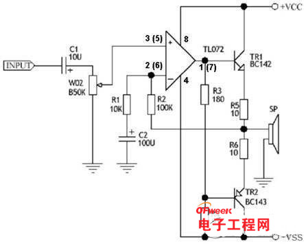
The circuit diagram is shown in Figure 1. The label of the right component of the headset is 100 added to the label of the left component. For example, R1 on the right is written as R101, C2 is written as C102, etc.
The amplifier here is essentially a boost amplifier. Its operational amplifier and output stage are class A. in order to realize direct coupling, the circuit adopts dual power supply.
First, the input signal is coupled to the volume control potentiometer VR1 through the DC blocking capacitor C1. The resistance value of VR1 is large, so that the sound is at the - 3dB point of the bass area (i.e. 2Hz).
For most signal sources, if its signal does not generate any additional DC voltage on the capacitor, the capacitor can not be used. Of course, it is best to keep the capacitor for safety, otherwise the DC offset at the input will cause a large offset at the output.
If the DC offset occurs and the value is small, the current consumption will be increased on the output stage, resulting in distortion; When the value is large, the headset will be damaged.
Volume control VR1 determines that the input impedance of the amplifier is 47K Ω, because the input stage of IC1 is a Junction FET (j.f.e.t), and its input impedance is about 10-12m Ω.
At present, there are a large number of operational amplifiers in the market, which can be widely used in audio circuits. However, after a large number of experiments, only tl072 has the best performance, reasonable price, low noise, response rate of 13V / MS and high current absorption capacity.
Although these components have many of the above characteristics, in fact, these components rarely operate under optimal conditions. For example, the operating current of the output stage of the operational amplifier is 2mA, which only works in class A and class B, and the load is less than 10k Ω. The solution is to connect a resistance with an appropriate value between the output end and the negative pole of the power supply, which forces it to be adjusted to class A.
The operational amplifier IC1 in the figure is connected to the in-phase input amplifier to connect the input signal from the sliding contact of the variable potentiometer VR1 to its homonymous terminal (+). Resistors R3 and R4 have two functions: the first function, as mentioned earlier, is to force the operational amplifier to work in class a state; The second function is to provide bias voltage for the output stage composed of Tr1 and TR2.
The complementary transistors Tr1 and TR2 adopt the working mode of emitter follower, so that the input impedance is high from the base and the output impedance of the output is low.
In circuit design, resistors R5 and R6 are very important, because R5 and R6 are connected in series with the emitters of Tr1 and TR2 to produce local negative feedback and make the output stage work in a linear state.
R5. The voltage drop on R6 and R3 is also very important. It makes the output stage enter class a working state. The negative feedback is fed back from the connection point of resistor R5 / R6 to the inverting input of IC1 through resistor R2 (pin 2). The voltage gain of the amplifier depends on the ratio (10 times) of resistors R2 and R1. Capacitor C2 is used to isolate DC, so that its AC negative feedback coefficient is R5 / R6, while DC negative feedback is 100%. The output of the amplifier is directly connected to the headset.
After introducing the circuit of the amplifier, attention should be turned to the power supply. The transformer has two 6V secondary coils, which can provide AC to the bridge rectifier. After rectification, filter with electrolytic capacitors C3 and C4. This is a very basic voltage stabilizing circuit. Of course, in order to achieve better results, you can also choose a better power supply mode. I believe it can be found in other circuits.
In daily life, when other family members are watching TV, or others are sleeping and can‘t be disturbed, you can‘t enjoy the beautiful music. In this case, we need to consider the amplifier introduced in this paper. Although the circuit is very simple, its high fax effect exceeds the standard power amplifier in the store. Using the tuner and answering machine movement, we can install a high-quality sound system, but the price is lower.
Design idea: before introducing the circuit in detail, let‘s talk about the design idea and explain how to achieve class a performance, and most experience sound power amplifiers use class B.
As we know, the output stage of a general amplifier consists of two branches: one branch processes the negative (negative half cycle) output signal, and the other branch processes the positive (positive half cycle) output signal. In this way, the static current can be minimized, but to drive the speaker, the voltage and current must have a large amplitude.
Unfortunately, these amplifiers have some distortion, called cross distortion. It appears at or near the zero crossing point of the output signal. If the two branches of the circuit are not completely matched, there will often be cross distortion, which makes the effect of listening to programs with headphones very poor.
Connecting the socket of the earphone to the output of the main amplifier also causes another problem: some resistors need to be connected in series between the earphone and the output stage to reduce the signal level. This will change the original negative feedback characteristics, which usually leads to a peak in the bass response, accompanied by a rapid roll down below the peak frequency.
In short, in order to produce an amplifier that can successfully drive headphones and obtain the best sound quality, the above two problems need to be solved.
To successfully design any kind of audio equipment, the first step is to find out what equipment is designed and determine its circuit. Ten years ago, the impedance of most earphones was 8 Ω, but now most of them use polyester diaphragm diaphragm, and the impedance is usually 32 Ω.
If you go to several high fax stores, you will find that the sensitivity of most products (including those with impedance of 8 Ω) is 87db-96db / MW, and the maximum input power is nearly 100MW. Through the test after installing this amplifier on 10 pairs of headphones, it is found that most headphones can output enough volume with input power of 10MW.
Class a power amplifier: for output power, the amplifier also needs low distortion, low noise and wide frequency band to meet the requirements of high fax equipment. To avoid cross distortion, the output stage must be class a amplifier.
Now let‘s talk about the ordinary small signal class a transistor amplification stage. In order to ensure the maximum dynamic range of the signal, the collector voltage should be half of the effective power supply voltage, and the current consumption of this level depends on the resistance value of the load connected to the collector. Ω is usually a power amplifier in a load of 8 Ω.
Now come back and look at the headphones. 560mwr is required to provide 10MW power for a pair of 32 Ω headphones M. S voltage dynamic range and current consumption of 25mA, so it can be realized as long as small signal transistors are used in the output stage. However, in fact, the maximum output power of the amplifier just exceeds 100MW. Before the highest output level of the amplifier, the headset has begun to appear distortion.
In order to make the output stage work normally, the operational amplifier is selected as the driver (its output stage is class a). Through the total harmonic distortion (THD) and bandwidth test of this headphone class a amplifier, the results are as follows:
THD<0.005%(1KHZ)
Frequency response: 2.5hz-100khz (- 3dB)
SNR: - 90dB
Maximum output: 120mW / 32 Ω
Circuit principle:
The circuit diagram is shown in Figure 1. The label of the right component of the headset is 100 added to the label of the left component. For example, R1 on the right is written as R101, C2 is written as C102, etc.
The amplifier here is essentially a boost amplifier. Its operational amplifier and output stage are class A. in order to realize direct coupling, the circuit adopts dual power supply.
First, the input signal is coupled to the volume control potentiometer VR1 through the DC blocking capacitor C1. The resistance value of VR1 is large, so that the sound is at the - 3dB point of the bass area (i.e. 2Hz).
For most signal sources, if its signal does not generate any additional DC voltage on the capacitor, the capacitor can not be used. Of course, it is best to keep the capacitor for safety, otherwise the DC offset at the input will cause a large offset at the output.
If the DC offset occurs and the value is small, the current consumption will be increased on the output stage, resulting in distortion; When the value is large, the headset will be damaged.
Volume control VR1 determines that the input impedance of the amplifier is 47K Ω, because the input stage of IC1 is a Junction FET (j.f.e.t), and its input impedance is about 10-12m Ω.
At present, there are a large number of operational amplifiers in the market, which can be widely used in audio circuits. However, after a large number of experiments, only tl072 has the best performance, reasonable price, low noise, response rate of 13V / MS and high current absorption capacity.
Although these components have many of the above characteristics, in fact, these components rarely operate under optimal conditions. For example, the operating current of the output stage of the operational amplifier is 2mA, which only works in class A and class B, and the load is less than 10k Ω. The solution is to connect a resistance with an appropriate value between the output end and the negative pole of the power supply, which forces it to be adjusted to class A.
The operational amplifier IC1 in the figure is connected to the in-phase input amplifier to connect the input signal from the sliding contact of the variable potentiometer VR1 to its homonymous terminal (+). Resistors R3 and R4 have two functions: the first function, as mentioned earlier, is to force the operational amplifier to work in class a state; The second function is to provide bias voltage for the output stage composed of Tr1 and TR2.
The complementary transistors Tr1 and TR2 adopt the working mode of emitter follower, so that the input impedance is high from the base and the output impedance of the output is low.
In circuit design, resistors R5 and R6 are very important, because R5 and R6 are connected in series with the emitters of Tr1 and TR2 to produce local negative feedback and make the output stage work in a linear state.
R5. The voltage drop on R6 and R3 is also very important. It makes the output stage enter class a working state. The negative feedback is fed back from the connection point of resistor R5 / R6 to the inverting input of IC1 through resistor R2 (pin 2). The voltage gain of the amplifier depends on the ratio (10 times) of resistors R2 and R1. Capacitor C2 is used to isolate DC, so that its AC negative feedback coefficient is R5 / R6, while DC negative feedback is 100%. The output of the amplifier is directly connected to the headset.
After introducing the circuit of the amplifier, attention should be turned to the power supply. The transformer has two 6V secondary coils, which can provide AC to the bridge rectifier. After rectification, filter with electrolytic capacitors C3 and C4. This is a very basic voltage stabilizing circuit. Of course, in order to achieve better results, you can also choose a better power supply mode. I believe it can be found in other circuits.
|
Disclaimer: This article is transferred from other platforms and does not represent the views and positions of this site. If there is infringement or objection, please contact us to delete. thank you! |


 Business consulting

 13823761625
 Mail me