


Using Complementary Tubes to Achieve Double Voltage and Back Voltage in DC-DC Converter
Time:2022-09-26
Views:1640
The circuit in this design idea makes use of an inherent characteristic of collector voltage in single transformer push-pull DC/DC converter: that is, their swing is twice of the power supply voltage. When these circuits are implemented with an NPN device, the collector swing is from 0V to twice the power rail voltage. When PNP devices are used, the collector voltage swing ranges from VCC to negative VCC with the same amplitude (Reference 1). In this circuit, a pair of complementary transistors drives two windings of the transformer, thereby simultaneously realizing a voltage multiplier and a negative voltage source.
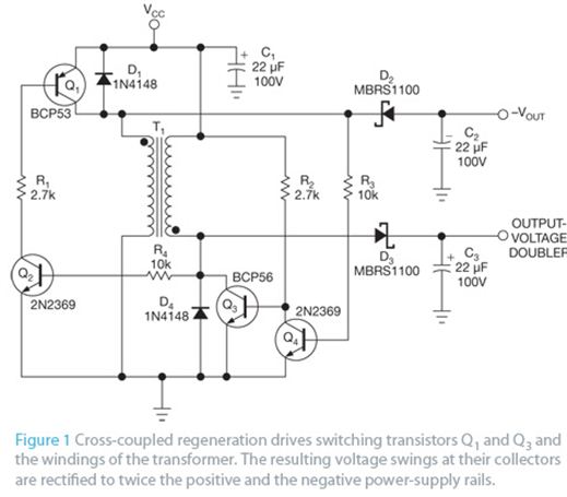
One winding of transformer T1 is grounded, which is driven by PNP transistor Q1 from VCC (Fig. 1). The other winding of T1 is connected to VCC, and NPN transistor Q3 drives its low end to ground. Q2 and Q4 drive Q1 and Q3 respectively. The collector of Q3 and Q1 provides cross coupling drive of Q2 and Q4 through the resistors R4 and R3. R1 and R2 form the collector loads of Q2 and Q4. D1 and D4 prevent the reverse breakdown of Q1 and Q3. The drive structure and the winding polarity of the transformer provide regenerative feedback and self oscillation, so that the transformer can alternately convert between positive saturation and negative saturation, generate the drive voltage, and make Q1 and Q3 turn on and off alternately.
1 Cross coupled regenerative drive switch transistors Q1 and Q3 and transformer windings. After the voltage swing obtained by the respective collector is rectified, twice the positive voltage and negative power rail are obtained.
The collector of Q1 generates a square wave with amplitude twice that of VCC, and its swing is from VCC to an equivalent but negative output voltage. At the same time, the collector of Q3 generates a square wave twice the voltage of the power rail, and its swing is from 0V to twice the voltage of the power rail.
D2 and C2 provide half wave rectification and filtering of Q1 collector waveform to generate negative voltage output. D3 and C3 are used for half wave rectification and filtering of Q3 collector waveform to obtain the output of voltage multiplier.
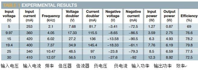
T1 is made of AWG 37 double stranded enamelled wire, which is wound on ferrite ring core for 200 turns in 1:1 (References 2 and 3). Table 1 shows the experimental results of the voltage multiplier and negative voltage generation circuit in the range of 5 to 30V input voltage, proving that the circuit can work with moderate efficiency in a wide input voltage range and output two power supplies at the same time.
Table 1 Experimental Results
|
Disclaimer: This article is transferred from other platforms and does not represent the views and positions of this site. If there is any infringement or objection, please contact us to delete it. thank you! |


 Business consulting

 13823761625
 Mail me