


Key Points of Design for DC-DC Switch Bucking Circuit
Time:2022-11-11
Views:1510
Buck circuit is a topology of DCDC switching converter. The design method is simple, but there are still many points for attention. Don‘t talk much nonsense, write directly.
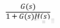
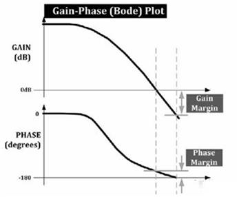
 The closed-loop transfer function of the step-down converter is: when the open-loop transfer function G (s) H (s) is - 1, the closed-loop transfer function will be infinite, that is, the phase of 0db in the Bode diagram of the amplitude of the open-loop threading function cannot be 180 °, otherwise the system will be unstable and cause oscillation. To ensure that the system will not oscillate when disturbed, certain phase margin and amplitude margin shall be reserved. Generally, the phase is set to 45 °, because under the 45 ° phase margin, the typical step response has only two rings, which can give consideration to both stability and response speed. Most of the current buck ICs do not reserve compensation interfaces externally, and the error amplifier will perform internal compensation. Since the compensation parameters are unknown, the feedback resistance should be selected according to the recommended parameters as far as possible. After the power supply is designed, the response of the power supply to the output dynamic load must be tested to observe the response speed and whether it is generated by ringing.
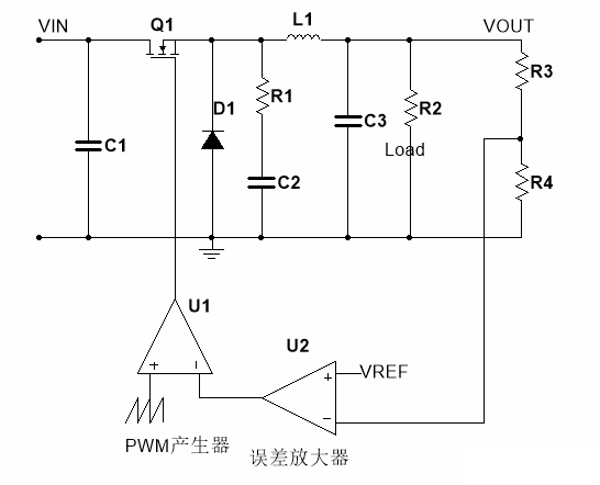
The structure of a common buck converter is shown in the figure. VIN is the DC input voltage, C1 is the input capacitor, Q1 is the MOSFET switch, D1 is the necessary diode in the buck structure, and D1 is also the MOSFET in the synchronous buck chip, which can improve efficiency and reduce costs. R1 and C1 are not necessary. RC absorption circuit can improve EMI performance. L1 is the energy storage inductance, C3 is the output capacitance, R3, R4, U2 and U1 form a feedback loop, and R3 and R4 set the output voltage.
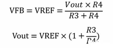
output voltage
Since the feedback voltage VFB is equal to the error amplifier reference voltage VREF, the output voltage can be obtained.
Feedback loop
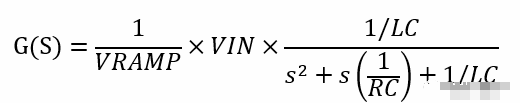
The transfer function from the control to the output of the step-down converter, where VRAMP represents the peak to peak value of the sawtooth wave at the in-phase input end of PWM generator U1, and R represents the output resistance, which is usually equivalent to the load resistance. C is the output capacitance.
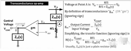
The transfer function of the feedback part of the buck converter can be divided into two types: traditional error amplifier and transconductance amplifier. The feedback resistance ratio of transconductance amplifier determines the gain and phase, and the same resistance ratio has the same gain and phase. In traditional operational amplifiers, the upper resistance affects the amplitude phase curve. To change the voltage, it is better to keep the upper resistance unchanged and change the lower resistance.
Input capacitance
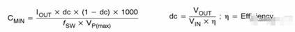
The purpose of the input capacitor is to reduce the input ripple, which should be controlled within 75mv (0.5%). Where, Cmin represents the minimum input capacitance, unit: uF; Iout represents the output current; Fsw is the switching frequency and VP (max) is the maximum peak to peak voltage of the input.
Input and output capacitance
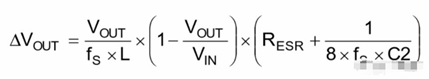
The output capacitor needs to maintain the DC output voltage. Ceramic, tantalum or low ESR electrolytic capacitors are recommended. Low ESR capacitors can better maintain low output voltage ripple. The output voltage ripple can be estimated according to the following formula:
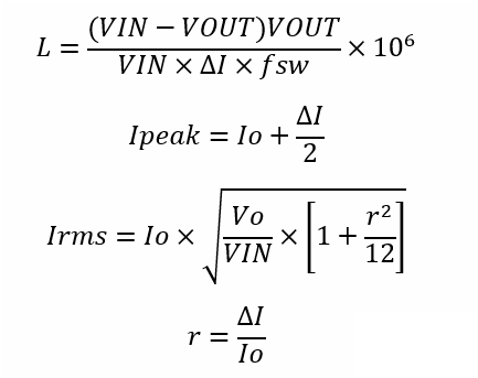
inductance
Inductance is the core component of the step-down circuit, which is related to the operation of the whole power supply. In the formula, IRIPPLE represents the ripple current of the inductor, which is the peak to peak value of the inductor current. Generally, 30% - 40% of the average inductance current is taken. The average inductance current of the step-down circuit is equal to the output current, and the unit of L is uH. Select the appropriate inductor and magnetic core according to the peak current of the inductor. The peak current must be less than the rated current of the inductor to ensure that the magnetic core is not saturated. Calculate the inductance loss and whether the heating is within the controllable range according to the effective value current of the inductance.
The above are the design points of DCDC switching step-down circuit. After the design, it is necessary to further test whether the output ripple, input ripple, inductance current and temperature meet the design value. PCB layout and wiring are also critical, affecting EMI and circuit performance. The design of RC buffer circuit and EMI control will not be repeated here due to the limited space of the article. Interested students can send messages to me through the official account and I will send references.
|
Disclaimer: This article is transferred from other platforms and does not represent the views and positions of this site. If there is any infringement or objection, please contact us to delete it. thank you! |


 Business consulting

 13823761625
 Mail me