


Burr free voltage monitor IC-concept or reality
Time:2022-12-06
Views:1378
Author: Suryash Rai, Engineer of ADI Core Product Business Unit
Reliable voltage monitor IC has always been the industry demand. Because it can improve system reliability and improve system performance in case of voltage transient and power failure. At present, semiconductor manufacturers are constantly improving the performance of voltage monitor IC to seek breakthroughs.
The monitor IC needs a minimum voltage called power on reset (VPOR) to generate a clear or reliable reset signal. Before the arrival of this minimum power supply voltage, the status of the reset signal is uncertain. Generally speaking, it is called reset burr.
The reset pin mainly has two different topologies, namely open drain and push-pull (Figure 1). Both topologies use NMOS as the pull-down MOSFET.
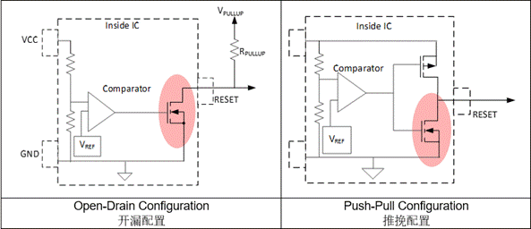
Figure 1 shows the open drain configuration and push-pull configuration of the reset topology
During power on, if the power supply voltage is lower than VPOR, there is not enough voltage to drive the internal MOSFET to work, so the MOSFET is closed. At this time, the monitor cannot control the reset voltage. The reset voltage will increase in proportion to the pull-up voltage (VPULLUP). Once the power supply voltage is higher than VPOR, the internal MOSFET will drive the RESET pin into a valid state.
Figure 2 shows how the reset voltage rises in proportion to the pull-up voltage (VPULLUP), which leads to the so-called reset burr.
The voltage monitor can be used to monitor the low power rails of FPGA, ASIC or DSP, and its voltage can be as low as 1V. In the low supply voltage processor, the logic level of I/O is very sensitive, and its VIH can be as low as 0.5V, as shown in Figure 3.
During power on, FPGA, ASIC or DSP should be in RESET state until all power rails are stable. When VDD is lower than VPOR, RESET pin may have burr, which may trigger the unknown state of FPGA. Once VDD is higher than VPOR, internal MOSFET will turn on and connect RESET to GND, and make RESET pin output correct logic low level.
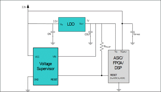
Figure 3 shows the interface between the monitor and ASIC/FPGA/DSP with low supply voltage
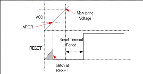
Figure 4 shows the power on sequence of the reset signal with burrs.
With the development of the electronics industry towards low-voltage semiconductor, analog chip manufacturers are also striving to achieve burr free monitors on the basis of traditional monitors. Manufacturers can reduce VPOR by improving the process, but a new architecture is required to achieve a true burr free monitor.
At present, system engineers use external circuits with traditional monitors to simulate the burr free monitoring function shown in Figure 5. This function can be achieved by adding a standard JFET configured as a source follower. The source voltage will depend on the difference between the gate voltage VG and the JFET threshold voltage. JFET threshold voltage will produce a voltage drop of about 1V between VG and VOUT, so as to prevent the output voltage of the monitor from rising when the internal MOSFET is turned off until the internal MOSFET of the monitor starts to work normally.
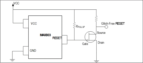
Figure 5 shows a traditional monitor with an external P-JFEF for burr free operation.
The real burr free monitor can draw current by resetting, even when VCC is zero, the reset pin will be forced to the ground potential. Figure 6 shows an example circuit for a true burr free monitor. ADI‘s MAX16161/MAX16162 can work without burrs without any external components, which is compact and economical.
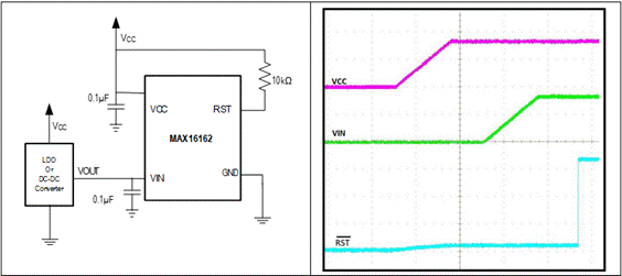
Fig. 6 Application diagram and corresponding sequence diagram of MAX16162
Summary:
The true burr free monitor IC is no longer just a concept. Designers now have a monitor IC that can generate a reliable reset signal under zero supply voltage, enabling system engineers to use the IC to monitor electronic devices with low supply voltage (below 1V). Moreover, the MAX16161/MAX16162 is a micro nanoPower IC with a quiescent current of only 825nA, which helps to extend the battery life of the system.
About the author
Suryash Rai has been at Maxim Integrated since 2016 ® (Now a part of ADI) as an application engineer, responsible for supporting voltage monitors and power protection products. He holds a Master‘s degree in Communication Engineering from the Karnataka National Institute of Technology. Suryash currently lives in Bangalore and enjoys cooking, traveling and making friends.
|
Disclaimer: This article is transferred from other platforms and does not represent the views and positions of this site. If there is any infringement or objection, please contact us to delete it. thank you! |


 Business consulting

 13823761625
 Mail me