


Principle Analysis of Buck Converter and Boost Converter
Time:2022-12-08
Views:1364
In the switching power supply, the power transistors in the DC converter work in the switching state. At present, the operating frequency of switching power supply is several hundred kHz, and some even reach the MHz level. The following figure shows the principle block diagram of DC-DC switching converter:
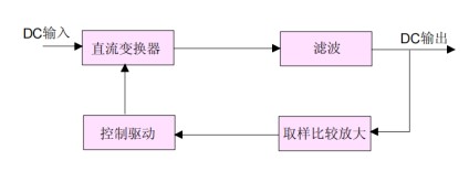
Principle block diagram of DC-DC switching converter
There are many ways to realize switching power supply, such as the most traditional pulse width modulation (PWM) technology, zero voltage (ZV), zero current (ZC) technology, phase-shift pulse width modulation zero voltage resonant transformation, etc. Under each technology, there are many kinds of topology structures. Switching power supply design requires rich knowledge of analog circuits, involving power device selection, power filter, drive circuit, control loop, high-frequency core transformer, EMC and many other aspects.
PWM
It is the most mature technology in switching power supply design. Pulse width modulation is a power control mode. The pulses with different duty cycles have different DC components. Therefore, when the load changes, the output voltage can be stabilized by adjusting the duty cycle of the output pulse. PWM is easy to realize, because the drive pulse has a fixed frequency and is independent of the load characteristics, so it is most widely used.
Buck circuit and boost circuit belong to PWM switching circuit, which are two basic circuits of DC/DC converter. Buck circuit switches are connected in series in the main circuit and are buck DC/DC converters. The switch tubes of the boost circuit are connected in parallel in the main circuit, which is a boost DC/DC converter.
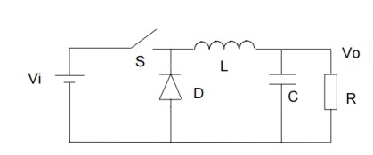
Buck converter
Buck converter is composed of voltage source, series switch and current load, which is also called series switch converter. The following figure shows its basic topology:
Buck converter
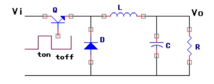
The following figure shows the circuit of transistor switching converter (buck), where transistor Q is a switching device, L is a filter inductor, C is a filter capacitor, and D is a freewheeling diode.
The transistor switching converter (buck) circuit ton is the conduction time of the transistor. During this time period, the current in L gradually increases. When the conduction is over, it enters the transistor cut-off time toff. At this time, because the current in L reaches the maximum ILmax, the current in the inductor cannot change suddenly, so there continues to be current flow in L, and diode D is used as the freewheeling element during the transistor cut-off. When the cut-off time is over, the current in the inductor reaches the minimum value ILmin, and the new cycle starts again.
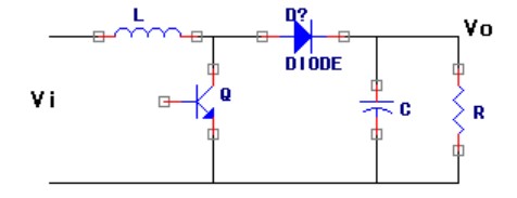
Boost converter
The Boost converter is obtained from the dual transformation of the buck converter. Its principle is shown in the following figure:
Boost converter
Boost converter is called parallel switching converter. Unlike the buck converter, the boost inductor is at the input (switch) and the buck inductor is at the output.
The output voltage Vo of Boost converter is always greater than the input voltage Vi. When the switch is on, diode D is closed, and the node voltage between inductor L and switch is 0. When the switch tube is closed, the potential at both ends of the inductor L is overturned, so the node voltage of the inductor L and the switch tube is greater than the input voltage Vi, and the inductance current flows continuously through the diode D, making Vo greater than Vi. It can be proved by Vo=Vi * [T/(T-Ton)] that T is the switching pulse period and Ton is the conduction time.
|
Disclaimer: This article is transferred from other platforms and does not represent the views and positions of this site. If there is any infringement or objection, please contact us to delete it. thank you! |


 Business consulting

 13823761625
 Mail me