


The Noise Source of Low Dropout LDO Regulator
Time:2022-12-17
Views:1525
Why noise sources are important
The importance of noise depends on its influence on the operation of the target circuit.
For example, a switching power supply has a significant output voltage ripple at 3 MHz. If the circuit it supplies only has a bandwidth of a few Hz, such as a temperature sensor, the ripple may not have any impact. However, if the switching power supply is powered by RF phase-locked loop (PLL), the results may be quite different.
In order to successfully design a robust system, it is important to understand the noise source, its spectrum characteristics, noise reduction strategies and the sensitivity of the target circuit to the noise.
This application note will also try to clarify the difference between power supply rejection ratio (PSRR) and endogenous noise, and explain how to apply the specifications of each parameter in the data manual.
noise source
Low dropout (LDO) regulators, or noise sources of any circuit, can be divided into two categories: internal noise and external noise. The internal noise is like the noise in your head, and the external noise is like the noise from a jet.
For electronic circuits, internal noise refers to the noise generated inside any electronic device, and external noise refers to the noise transmitted from the outside of the circuit to the circuit.
LDO is easy to use, but PSRR and endogenous noise are often confusing. In many cases, they are simply classified as noise together, which is a misuse of performance indicators, because the two types of noise have different characteristics, and the methods used to reduce their impact on system performance are also different.
Figure 1 is a simple block diagram of LDO, showing the difference between internal and external noise sources. The error amplifier determines the PSRR of LDO, and therefore its ability to suppress input noise. Internal noise always appears at the output of LDO.
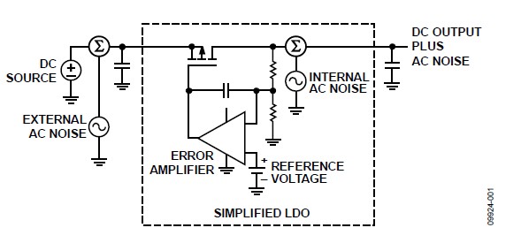
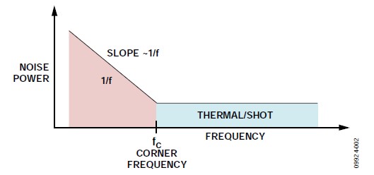

Figure 1. Simplified LDO block diagram showing internal and external noise sources
Internal noise
There are many sources of internal noise, and various noise sources have their own unique characteristics. Figure 2 shows how the noise of a typical device changes with frequency and the contribution of various noises to the total noise. The transition point from the 1/f region to the hot region is called the transition frequency. The internal noise mainly includes the following categories: thermal noise, 1/f noise, shot noise, popping or popcorn noise.
Figure 2. Relationship between typical noise power and frequency
thermal noise
At any temperature above absolute zero, the carriers (electrons and holes) in conductors or semiconductors will be disturbed, which is the source of thermal noise (also known as Johnson noise or white noise). Thermal noise power is proportional to temperature. It is random and therefore does not change with frequency.
Thermal noise is a physical process, which can be calculated by the following formula:
Including:
K is the Boltzmann constant (1.38-23 J/K).
T is the absolute temperature (K=273 ° C).
R is the resistance in Ω.
B is the bandwidth of the observed noise (in Hz, the RMS voltage measured on the resistance is also a function of the bandwidth being measured).
For example, the noise added to the circuit by a 100 k resistor at 1 MHz bandwidth and room temperature is:

1/f noise
1/f noise comes from surface defects of semiconductor. The 1/f noise power is proportional to the bias current of the device and inversely proportional to the frequency, which is different from thermal noise. This inverse characteristic holds even if the frequency is very low. However, when the frequency is higher than several kHz, the relationship curve is almost flat. 1/f noise is also called pink noise because its weight is relatively high at the low end of the spectrum.
1/f noise mainly depends on device geometry, device type and semiconductor materials. Therefore, it is extremely difficult to create its mathematical model. Generally, empirical tests in various situations are used to characterize and predict 1/f noise.
In general, the 1/f noise of devices with embedded junctions, such as bipolar transistors and JFETs, is often lower than that of surface devices such as MOSFETs.
Shot noise
The shot noise occurs in places with potential barriers, such as PN junctions. The current in semiconductor devices has quantum properties, and the current is not continuous. When the charge carriers, holes and electrons cross the potential barrier, shot noise will be generated. Like thermal noise, shot noise is random and does not change with frequency.
Popping or popcorn noise Popping or popcorn noise is a low-frequency noise that seems to be related to ion pollution. Popcorn noise is characterized by a sudden shift of the bias current or output voltage of the circuit, which lasts for a short time, and then the bias current or output voltage suddenly returns to its original state. This offset is random, but appears to be proportional to the bias current and inversely proportional to the square of the frequency (1/f2).
Due to the high cleanliness of modern semiconductor technology, the burst noise has almost been eliminated and is no longer a major factor in device noise.
External noise
External noise sources are far more than internal noise sources, including the following categories:

● Electromagnetic fields coupled to sensitive circuits.
● Mechanical shock or vibration that causes piezoelectric materials to interfere with AC voltage.
● Noise from other circuits conducted or radiated to the circuit through power supply or poorly designed PCB layout and wiring.
electromagnetic coupling
The electromagnetic field can induce noise in the circuit by one or more of the following methods:
Radiation coupling, capacitive coupling, inductive coupling and conductive coupling. The impact of such coupling can be reduced through proper PCB layout and shielding technology, but this is beyond the scope of this application note.
Piezoelectric effect
Some devices, such as high capacitance multilayer ceramic capacitors, are sensitive to mechanical shock and vibration (i.e., have chattering noise effect), because of the use of high dielectric constant materials in their structures. These dielectrics have high voltage electrical properties and can easily convert tiny mechanical vibration into millivolt or even microvolt level signals. Therefore, it is not recommended to use high capacitance ceramic capacitors in low-level signal link circuits.
Although the film capacitance is not piezoelectric, it is also sensitive to vibration, because any mechanical stress on the film dielectric will cause slight changes in the film thickness, resulting in a slight increase or decrease in capacitance. The energy stored in the capacitance is constant, so the voltage must be changed slightly to accommodate the capacitance change. The relationship among energy, capacitance and voltage can be described by the following formula:
After the mechanical stress is removed, the voltage on the capacitor returns to its original state. If the mechanical stress is periodic, a small AC voltage will be generated.
Power noise
Power supply noise and ripple are generally the most important noise sources at the LDO output, next only to the internal noise. LDO can greatly improve the power quality of the downstream circuit according to the spectrum composition of the noise source.
In many systems, the power supply from the AC power supply or battery is converted from the high efficiency switching mode power supply to the intermediate voltage for distribution throughout the system. These intermediate voltages are converted to specific voltages at the point of use.
The noise of switching mode power supply mainly depends on its topology and load state.
The spectrum components can range from a few Hz to tens of MHz In many cases, in order to power sensitive analog loads, it is necessary to purify the high noise power distribution bus through LDO. The ability of LDO to suppress input source noise depends on its PSRR and how it varies with frequency.
Noise in LDO
The main internal noise sources of LDO are internal reference voltage and error amplifier.
Modern LDOs operate with tens of nA of internal bias current to achieve 15 μ A or less quiescent current. This low bias current requires the use of large bias resistors up to class G.
Reference voltage noise
The thermal noise of the resistance is defined as Vn=√ (4kTRB). It can be seen that the resistance may contribute considerably to the noise of the reference voltage circuit. Fortunately, the reference voltage of LDO does not require bandwidth above several Hz, and the noise can be easily reduced by using on-chip passive filtering.
For example, a bandgap reference voltage source with a source impedance of 0.1 G Ω has 407 in the range of 10 Hz to 100 kHz μ The noise of V rms, which limits the bandwidth to 10 Hz, can be reduced to 4.1 μ V rms. If the bandwidth is reduced to 1.6 Hz, the noise contribution of the reference voltage source is reduced to 1.3 μ V rms. A single pole RC filter with a turning frequency of 1.6 Hz can be constructed by using a 1 G Ω resistor and a 100 pF capacitor. Figure 3 shows how to implement such a 1.0V ultra-low noise reference voltage source in the chip.
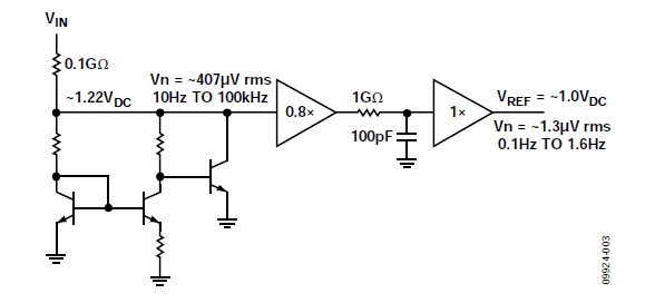
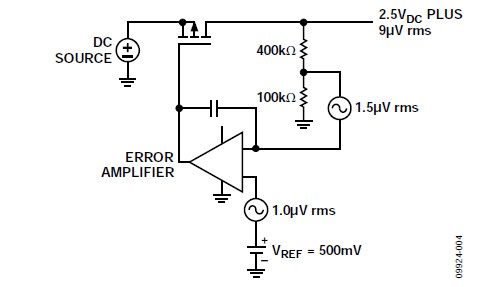
Figure 3. Ultra low noise, ultra-low power reference voltage source (ADP223)
Error amplifier noise
If a low noise reference voltage source is used, the error amplifier will become an important source of total output noise. The noise contributions of the reference voltage source and the error amplifier are not related, and must be summed by the root mean square method.
Figure 4 shows an example of a 2.5 V output LDO with a 500 mV reference voltage source. The noise of the reference voltage source is 1 μ V rms, noise of error amplifier is 1.5 μ V rms, total noise 9 μ V rms, calculated as follows:
Figure 4. Noise contribution of reference voltage source and error amplifier (ADP223).
Reduce LDO noise
There are two main methods to reduce LDO noise:
● Filter the reference voltage
● Reduce noise gain of error amplifier
Some LDOs allow the use of external capacitors to filter the reference voltage. In fact, many so-called ultra-low noise LDOs require external noise reduction capacitors to achieve their low noise performance. The disadvantage of external filtering of the reference voltage is that the starting time is proportional to the size of the filter capacitor. Figure 3 illustrates why this is the case. The node connecting the 100 pF capacitor is led out to connect the external capacitor.
Reducing the noise gain of the error amplifier has less influence on the starting time than filtering the reference voltage, so it is easier to balance the starting time and output noise. Unfortunately, for a fixed output LDO, the output noise cannot be reduced generally because the feedback node cannot be accessed. However, in most adjustable output LDOs, it is easy to access feedback nodes.
If the noise contribution of the error amplifier is greater than that of the reference voltage source, reducing the noise gain of the error amplifier can significantly reduce the total noise of the LDO. One way to determine whether an error amplifier is the main source of noise is to compare the noise of a fixed output version of a particular LDO with that of a tunable output version. If the noise of fixed output LDO is much lower than that of adjustable output LDO, the error amplifier is the main noise source.
Figure 5 shows a 2.5V output adjustable LDO with R1, R2, R3 and C1 as external components. The R3 selected is used to set the high frequency gain of the amplifier to 1.5 to 2 times. Some LDOs have low phase margins or are unstable at unity gain. The selected C1 is used to set the low frequency zero point of the noise reduction network (C1, R1 and R3) within the range of 10 Hz to 100 Hz, so as to ensure that the noise in the 1/f zone is fully reduced.
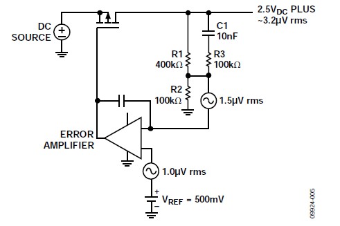
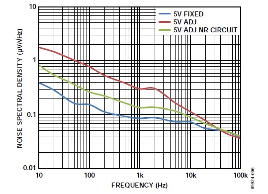
Figure 5. Reducing Noise Gain of Adjustable Output LDO
Figure 6 shows the influence of noise reduction (NR) network on the noise spectral density of high-voltage adjustable LDO. As can be seen from Figure 6, in the range of 20 Hz to 2 kHz, the noise performance is improved by about 3 times (~10 dB). Note that the two curves are fused above 20 kHz, because the closed-loop gain of the error amplifier reaches the open-loop characteristic of the amplifier, which cannot further reduce the noise gain.
In the same frequency range, PSRR performance is also improved (see "Improving PSRR" for more information).
Figure 6. Noise spectral density of adjustable output LDO
Noise specifications in LDO Data Book
In general, the LDO data book specifies internal noise in two ways:
● Total integrated noise within a certain bandwidth, expressed in V rms (see Figure 7)
● Noise spectral density curve. The relationship between noise and frequency is expressed in V/Hz (see Figure 6). The ADI data manual specifies the total integrated noise within the bandwidth of 10 Hz to 100 kHz. Figure 7 shows the relationship between the total RMS noise of ADP223 at different output voltages and the load current in the 10 Hz to 100 kHz bandwidth.
In general, the RMS noise under light load is low, because the bandwidth of LDO decreases with the quiescent current. When the load current reaches several mA, LDO operates with full bandwidth, and the noise does not change with the load.
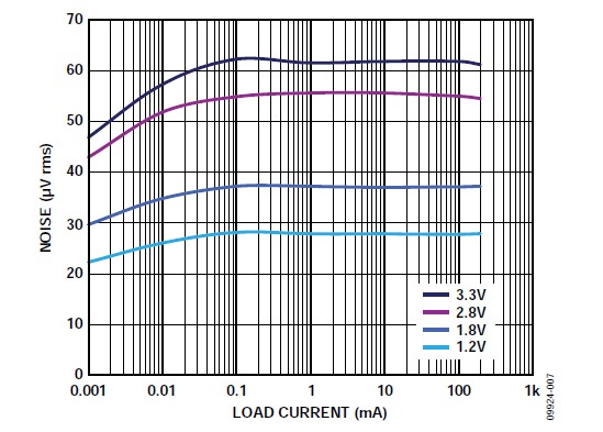
Figure 7. RMS Noise vs. Load Current and Output Voltage (ADP223)
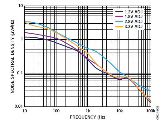
Figure 8 shows the noise spectral density diagram of ADP223, which shows the change of noise spectral density with output voltage in the frequency range of 10 Hz to 100 kHz.
The root mean square noise can be obtained by integrating the data in this graph within this bandwidth.
For any frequency range, the root mean square noise can be estimated using the following formula:


Including:
BW = NFU -NFL
NFL is the noise at the lower frequency limit (unit: μ V/√Hz)。
NFU is the noise at upper frequency limit (unit μ V/√Hz)。
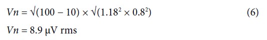
For example, for the 1.2 V output in Figure 8, the RMS noise in the range of 10 Hz to 100 Hz is about:
The noise spectrum density is measured at a sufficiently high load current to ensure that the LDO operates at full bandwidth, but it cannot be too high to cause serious self heating effects. For most LDOs with a maximum output current of 1 A or less, 10 mA is appropriate.
Figure 8. Relationship between noise spectral density and output voltage (ADP223)
Compare LDO noise indicators
The root mean square noise is represented by a single number, so it is a useful indicator for comparing the performance of different LDOs. However, the noise index of the LDO to be compared must be measured under the same test conditions.
For example, in the range of 10 Hz to 100 kHz, the ADP223 root mean square noise of 1.2 V output is about 27.7 μ V rms. If the noise bandwidth is reduced to 100 Hz to 100 kHz, the RMS noise is reduced to about 26.2 μ V rms. The root mean square noise is reduced because the noise measurement no longer includes 8.9 in the range of 10 Hz to 100 Hz μ V rms noise.
In addition, attention must be paid to the noise reduction characteristics of the LDO under consideration. For LDOs that require external capacitors for noise reduction, the noise may be 100 times higher when capacitors are not used than when capacitors are used. In applications requiring small size and low cost, in order to save PCB area and cost, it is possible to choose LDOs that do not need external noise reduction capacitors, but whose noise is slightly higher than that of those that need noise reduction capacitors
LDO PSRR
The PSRR of LDO is often confused with internal noise. In short, PSRR measures the ability of the circuit to suppress external signals (noise and ripple) at the power input, so that these interference signals will not damage the circuit output. The PSRR of the circuit is defined as follows:
VEIN and VEOUT are the external signals at the input and output respectively.
For ADC, DAC, amplifier and other circuits, the PSRR is applicable to the input terminals that supply power to the target circuit. For LDO, the input power supply pin supplies power to the regulated output voltage and internal circuit.
Relationship between PSRR and frequency
PSRR is not defined by a single value because it is frequency dependent. As shown in Figure 1, LDO is composed of power adjusting elements such as reference voltage, error amplifier, MOSFET or bipolar transistor. The error amplifier provides DC gain to adjust the output voltage. The AC gain characteristics of the error amplifier largely determine the PSRR of the LDO. A typical LDO may have a PSRR of up to 80 dB at 10 Hz, but it may drop to only 20 dB at tens of kHz
The relationship between gain bandwidth of error amplifier and PSRR is shown in Figure 9. This example has been highly simplified, and the parasitic effects of output capacitance and adjusting elements have been ignored.
PSRR is equal to the reciprocal of 60 dB open-loop gain until the gain begins to roll off at 3 kHz. PSRR decreases at a rate of 20 dB/10 times until PSRR reaches 0 dB at 3 MHz; PSRR remains 0 dB for all higher frequencies thereafter.
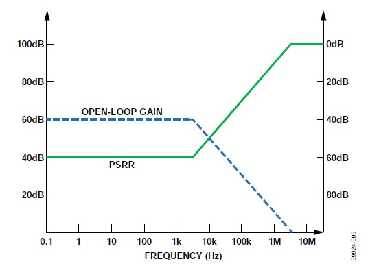
Figure 9. Simplified LDO gain versus PSRR
The PSRR curve in Figure 10 shows three main frequency domains characterizing LDO PSRR:
Reference voltage PSRR area, open loop gain area and output capacitance area.
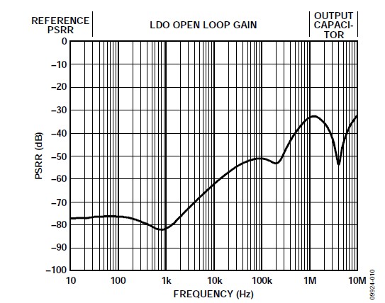
Figure 10. Typical LDO PSRR vs. Frequency
The reference voltage PSRR area depends on the PSRR and LDO open-loop gain of the reference voltage amplifier. Ideally, the reference voltage amplifier is completely unaffected by power supply disturbances. In fact, the reference voltage only needs to suppress power noise up to tens of Hz, because the error amplifier feedback ensures high PSRR at low frequencies
In the second region above about 10 Hz, PSRR is mainly determined by the open-loop gain of LDO. The PSRR in this area is a function of the gain bandwidth of the error amplifier (the highest is the unit gain frequency). At low frequencies, the AC gain of the error amplifier is equal to the DC gain and remains constant until the 3 dB roll off frequency is reached. At the frequency higher than the 3dB roll off point, the AC gain of the error amplifier decreases with the increase of the frequency, and the change rate is usually 20 dB/10 times.
Above the unit gain frequency of the error amplifier, the feedback of the control loop has no effect on the PSRR, which is determined by the output capacitance and any parasitic effect between the input and output voltages. At these frequencies, the output capacitors ESR and ESL as well as the circuit board layout and routing will strongly affect PSRR. In order to reduce the impact of high-frequency resonance, special attention must be paid to the layout and routing.
Relationship between PSRR and load current
As described in the section "Relationship between PSRR and frequency", the PSRR of LDO depends on the gain bandwidth of the feedback loop of the error amplifier. Any factor that affects the gain of this loop will affect the PSRR of LDO. The load current can affect the PSRR in two ways
Under low load current (usually less than 50 mA), the output impedance of the adjusting element is very high. Due to the negative feedback of the control loop, the LDO output seems to be an ideal current source. The poles formed by the output capacitors and the adjusting elements cause the output impedance to appear at relatively low frequencies, and often increase the PSRR at low frequencies The high DC gain of the output stage at low current also tends to improve the PSRR at frequencies below the unity gain point of the error amplifier
Under heavy load current, LDO output is not very like an ideal current source, and the output impedance of the adjusting element is relatively low, resulting in a decrease in the gain of the output stage. The decrease of output stage gain makes the PSRR in the unit gain frequency range from DC to feedback loop decrease. Figure 11 shows that the DC gain decreases significantly as the load current decreases. From 200 mA to 100 mA, the DC gain of ADP151 decreases by more than 20 dB
The bandwidth of the output stage is increased due to the increase of the output pole frequency. In high frequency, it seems that PSSR should be improved with the increase of loop bandwidth, but in fact, due to the reduction of total loop gain, high-frequency PSRR may not be improved. Generally speaking, PSRR under light load is better than that under heavy load
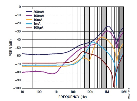
Figure 11. Relationship between typical LDO PSRR and load current (ADP151)
Relationship between PSRR and LDO margin
The PSRR of LDO is also related to the differential pressure or margin from input to output. For fixed margin voltage, PSRR decreases with the increase of load current, which is especially obvious when the load current is heavy and the margin voltage is small. Figure 12 shows the PSRR difference of 2.8 V output ADP151 under 200 mA load, 500 mV and 1 V margin.
With the increase of load current, the adjusting element (P-MOSFET of ADP151) is out of saturation state and enters the three pole working area. Its gain decreases accordingly, which leads to the decrease of the total loop gain of LDO and thus the decrease of PSRR. The smaller the margin, the greater the gain reduction. In some small margin voltages, the control loop has no gain at all, and the PSRR is reduced to 0
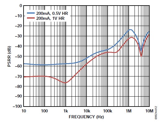

Figure 12. Typical LDO PSRR versus margin (ADP151).
Another factor that reduces the loop gain is that the adjusting element has a non-zero resistance, or RDSON RDSON includes MOSFET on resistance, on-chip interconnect resistance and wire solder resistance. RDSON is estimated by the differential voltage of LDO. For example, the worst case differential voltage of the WLCSP packaged ADP151 under 200 mA load is 200 mV, which means that RDSON is about 1.0 Ω. Figure 13 shows a simplified schematic of the adjusting element and RDSON.
Figure 13. Simplified LDO display adjustment element resistance
Any voltage drop on the RDSON caused by the load current will cause the margin of the effective part of the adjusting element to decrease by a corresponding amount. For example, if the adjusting element is a 1-component and the load current is 200 mA, the margin will be reduced by 200 mV. When LDO operates at 1 V or lower margin voltage, this voltage drop must be considered when estimating LDO PSRR.
Improve PSRR
Under the given load current, the PSRR of LDO can be improved in many ways:
● Let the LDO operate with a margin of at least 1 V. Some LDOs, such as ADP151, can work well with margins as low as 500 mV.
● Use LDO whose maximum load current rating is at least 1.5 times greater than the expected load
● Add external filtering at the input or output of LDO.
● If the margin is sufficient, cascade two or more LDOs
Add external filtering to improve PSRR
The PSRR of LDO circuit can be greatly improved by adding external filter, but the cost is that the circuit is more complex, and the margin and efficiency will be reduced. Depending on the application, additional filtering can be added to the input (pre filtering) or output (post filtering) of the LDO.
Post filtering is often used when there is significant low frequency noise at the LDO output. Modern low noise LDO such as ADP151 no longer need post filtering. The disadvantage of post filter is that the resistance of filter inductance will cause additional load adjustment error.
When high frequency noise must be suppressed, such as output voltage ripple of switching converter, it is more appropriate to add pre filter, and it will not affect load adjustment.
Figure 14 shows that a LDO circuit uses both pre filter and post filter, however, usually only one external filter is used.
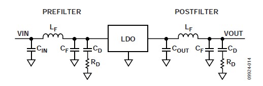
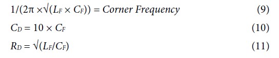
Figure 14. LDO with external pre filter and post filter
The main elements of the filter are LF and CF, which are used to set the turning frequency of the filter. CD and RD eliminate the resonance of LF and CF. CIN and COUT are typical input and output capacitors for LDO, but CIN is not required.
The values of CF, LF, CD and RD can be determined by the following equation:
For example, if it is necessary to reduce the 1 MHz ripple of a switching converter by at least 30 dB, a transition frequency of 100 kHz to 200 kHz should be sufficient.
Assume CF=1 according to equation 9 μ F、LF = 1 μ H. Then fC=160 kHz
CD=10 according to equation 10 μ F; According to equation 11, RD=1 Ω.
Figure 15 shows the response of an example filter. The attenuation is about 33 dB at 1 MHz and the maximum peaking is about 0.7 dB at 81 kHz.
The DC resistance of the inductor LF shall be as low as possible to minimize the margin reduction (for the post filter, the load adjustment error shall be minimized). The saturation current of the inductor must also be at least as high as the maximum expected load current of the circuit.
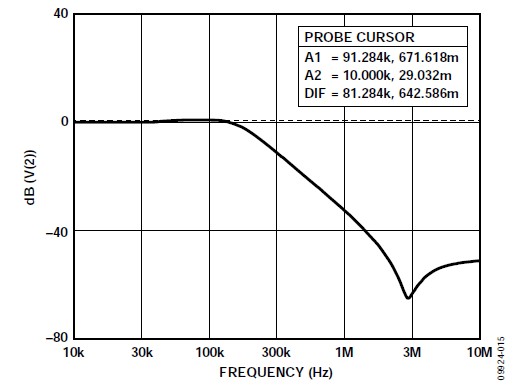
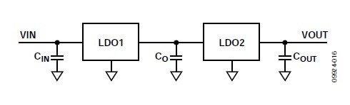
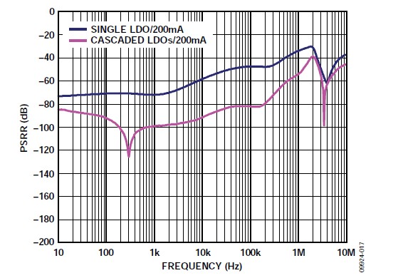
Figure 15. Response of an example ripple filter
Cascade multiple LDOs to improve PSRR
In applications with sufficient margin, cascading multiple LDOs (such as ADP151) can greatly improve PSRR while maintaining the low output noise characteristics of ADP151. Figure 16 shows the schematic diagram of two cascaded LDOs. The bypass capacitors CIN, COUT and CO are equal to the recommended values in ADP151 data manual, i.e. 1 μ F.
Figure 16. Cascaded LDO
The selected LDO1 output ensures that the margin on LDO2 is at least 500 mV. To obtain the best performance, the margin on LDO1 should also be at least 500 mV. Figure 17 compares the PSRR of a 1.8 V ADP151 with that of two cascaded ADP151. The load current and margin in both cases are 200 mA and 1 V. It can be clearly seen from Figure 17 that the PSRR in a wide frequency range can be increased by up to 30 dB by cascading two LDOs
Figure 17. PSRR of one LDO and cascaded LDO
Compare LDO PSRR indicators
When comparing the PSRR indexes of LDO, ensure that the measurement is conducted under the same test conditions. Many older LDOs only describe PSRR at 120 Hz or 1 kHz, without mentioning margin voltage or load current. At least the PSRR in the electrical specification sheet shall be listed for different frequencies. In order to make the comparison meaningful, it is better to use the typical operating performance curve of PSRR under different loads and margin voltages.
Output capacitance will also affect LDO PSRR at high frequency For example, 1 μ The impedance of F capacitor is 10 μ F 10 times the capacitance. When the frequency is higher than the 0 dB crossover frequency of the error amplifier, the attenuation of power supply noise is related to the output capacitance, and the capacitance is particularly important at this time. When comparing PSRR values, the type and value of output capacitance must be the same, otherwise the comparison is invalid.
Total LDO noise
Both internal noise and PSRR form part of the total output noise of LDO. Depending on the application, the contribution of either internal noise or PSRR may be important, or both. When both PSRR and endogenous noise have an impact on the overall performance of the application, a single value of noise cannot be applied.
A typical application is to use a switching converter to power the RF PLL. To suppress the ripple from the switching converter, the output is regulated by an LDO.
The internal noise of LDO will slightly modulate the power supply of PLL, thus causing phase noise at the output of PLL. The phase noise of PLL is caused by VCO frequency offset and is related to the power supply voltage. It is expressed as △ f/△ V and is often referred to as VCO shift gain.
The PSRR of LDO can reduce the noise of switching converter below the unit gain frequency of LDO. When the unit gain frequency of LDO is exceeded, the switching converter noise is attenuated by the LDO output capacitor or passive filter after LDO. The frequency harmonics of switching converter without sufficient attenuation are shown as spurious at either end of PLL frequency.
Concluding remarks
Generally speaking, LDO noise includes two parts: internal or endogenous noise and external or exogenous noise.
Thermal noise and 1/f noise are the main endogenous noise sources, which are related to LDO design and semiconductor technology.
There are many sources of external noise, but the most common is LDO input power noise.
Since LDO has high gain to ensure good line and load adjustment performance, it can attenuate noise and ripple from the input power supply, which is the PSRR of LDO The bandwidth of LDO is limited, so its PSRR decreases with the increase of frequency. The noise outside the LDO bandwidth cannot be attenuated by the LDO itself, so passive filters can be used to reduce it.
|
Disclaimer: This article is transferred from other platforms and does not represent the views and positions of this site. If there is any infringement or objection, please contact us to delete it. thank you! |


 Business consulting

 13823761625
 Mail me