


Design and Implementation of Interlaced Low-voltage and High-current DC-DC Converter
Time:2023-03-04
Views:1138
1 Introduction
In recent years, as the input voltage requirements of computer microprocessors become lower and lower, the research of low-voltage and high-current DC-DC converters has attracted the attention of many researchers, and various topologies emerge in endlessly. Synchronous rectification technology, multi-phase technology, magnetic integration technology, etc. are also applied in this field. In this paper, a low voltage high current DC-DC converter with interleaved parallel connection is proposed. Its primary side adopts symmetrical half-bridge structure, and its secondary side adopts current-doubling rectifier structure. This structure can greatly reduce the current ripple on the filter capacitor, thus greatly reducing the size of the filter inductor and the size of the entire DC-DC converter. This converter operates in the environment of 48V input voltage and 100kHz switching frequency.
Structure Analysis of Low-voltage and High-current DC-DC Converter with Double Current Rectification
The circuit schematic diagram of low voltage high current DC-DC converter with current-doubling rectifier is shown in Figure 1. The symmetrical half-bridge structure is adopted at the primary side and the current-doubling rectifier structure is adopted at the secondary side. When S1 is on, SR1 must be cut off and L1 charged; When S2 is on, SR2 must be cut off and L2 charged, so that the filter inductance current will be shifted and superimposed on the filter capacitor. Figure 2 shows the switch control strategy.
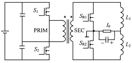
Figure 1 Circuit schematic diagram of low-voltage high-current DC-DC converter with current-doubling rectifier
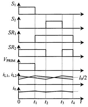
Figure 2 Control strategy of switch
It can be seen from the above analysis that the current of the two filter inductors on the secondary side of the current-doubling rectifier structure is superimposed on the filter capacitor, which makes the output current ripple become relatively small.
The synchronous rectifier in the structure is driven and processed according to the external signal, which makes the control very complex. However, it is difficult to use a simple self-drive method in this half-bridge-doubling topology. Because in this structure, if the appropriate point is directly taken from the circuit as the drive signal of the synchronous rectifier, the synchronous rectifier will stop when the drive signal is zero in the dead time. In order to use the self-drive mode in the half-bridge current-doubling topology, the auxiliary winding must be used.
Taking a single half-bridge-current doubling topology as an example, see Figure 3. VSEC is the secondary side voltage of the transformer and Vgs is the drive voltage of the synchronous rectifier obtained by the auxiliary winding. It can be seen that even in the dead time, the drive voltage of the synchronous rectifier cannot be zero, which ensures the application of the self-drive mode in this topology.
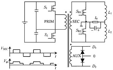
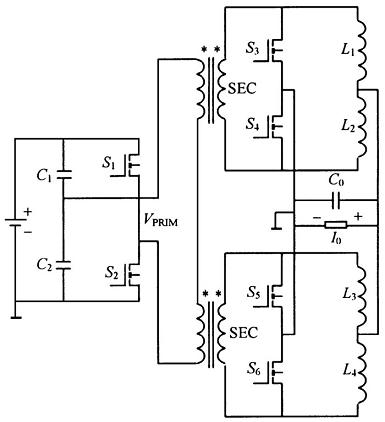
Figure 3 Self-driving synchronous rectifier circuit and waveform diagram
In addition, because the MOSFET conduction voltage drop will increase under the condition of large current, resulting in large conduction loss, so multiple MOSFETs should be used in parallel to reduce the loss.
3 interleaved parallel low voltage high current DC-DC converter
3.1 Circuit schematic diagram
To sum up, the current-doubling rectifier low-voltage high-current DC-DC converter has good performance. On this basis, the staggered parallel technology is introduced to form a new structure, called parallel low-voltage high-current DC-DC converter, which can further reduce the output current ripple.
Figure 4 shows the circuit schematic diagram of the interleaved low-voltage high-current DC-DC converter (taking the simplest two current-doubling rectifiers interleaved in parallel as an example).
Figure 4 Circuit schematic diagram of interleaved low-voltage high-current DC-DC converter
3.2 Switching control strategy of converter
The switching control strategy of the interleaved low-voltage high-current DC-DC converter is shown in Figure 5.
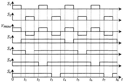
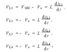
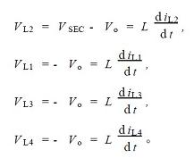
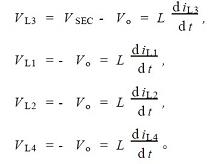
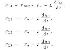
Figure 5 Switching control strategy of interleaved low-voltage high-current DC-DC converter
3.3 Performance of interleaved low-voltage high-current DC-DC converter
First of all, the greatest advantage of this topology is that the structure of the primary side of the transformer is simplified, and the control becomes very simple. Secondly, the realization of this method must adopt synchronous rectification circuit, because the realization of interleaved parallel circuit requires that the upper and lower potentials of the secondary side of the transformer are positive in turn, and there is only one positive potential in a period of time, and the rest are zero potential. However, in this topology, because the primary side of the two transformers is connected in series and the secondary side is connected in parallel, if the Schottky diode is used as a rectifier, the input voltage will be divided on the primary side of the two transformers, and the Schottky diode has no gating function, so the waveform of the secondary side of the transformer will be completely symmetrical, and the current of the upper and lower rectifier circuits are completely coincident, which can not achieve the purpose of current interleaving and paralleling.
In this way, synchronous rectifier is used to complete this function, and the bidirectional conductivity of MOSFET is also used, because the leakage source current of synchronous rectifier is distributed on both sides of the horizontal axis of the coordinate. The process of this structure is detailed as follows:
1) S1 is on, S2 is off; S3 cut-off, S4, S5 and S6 are all on. Due to the conduction of S4, S5 and S6, the lower end of the secondary winding of the first transformer is at zero potential, and the upper and lower ends of the secondary winding of the second transformer are at zero potential. The current on the inductance L1 rises, and the current on L2, L3 and L4 drops.
2) S2 is on, S1 is off; S4 cut-off, S3, S5 and S6 are all on. Due to the conduction of S3, S5 and S6, the upper end of the secondary winding of the first transformer is at zero potential, and the upper and lower ends of the secondary winding of the second transformer are at zero potential. The current on the inductance L2 rises, and the current on L1, L3 and L4 decreases.
3) S1 is on, S2 is off; S5 cut-off, S3, S4 and S6 are all on. Due to the conduction of S3, S4 and S6, the lower end of the secondary winding of the second transformer is at zero potential, and the upper and lower ends of the secondary winding of the first transformer are at zero potential. The current on inductance L3 rises, and the current on L1, L2 and L4 decreases.
4) S2 is on, S1 is off; S6 cut-off, S3, S4 and S5 are all on. Due to the conduction of S3, S4 and S5, the upper end of the secondary winding of the second transformer is at zero potential, and the upper and lower ends of the secondary winding of the first transformer are at zero potential. The current on the inductance L4 rises, and the current on L1, L2 and L3 decreases.
The voltage drop of the rectifier is ignored for the above types, and VSEC is the voltage value at the secondary side of the transformer.
According to the above analysis, this interleaved half-bridge current-doubling topology can be realized by applying synchronous rectifier through the method of series connection of the primary side and parallel connection of the secondary side of the transformer. Its advantages mainly include the following aspects:
1) It effectively simplifies the topology and control strategy.
2) If the peak-to-peak value of the ripple is constant while the frequency is constant, this structure can effectively reduce the value of the filter inductance, thus speeding up the dynamic response time of the whole converter.
3) Compared with the non-staggered half-bridge-current doubling topology, the conduction loss of the primary side and the secondary side is not much different. However, due to the use of the interleaved parallel technology, the switching frequency of the secondary side is half of the original, and the corresponding switching loss is also half of the original. Since the switching loss of the converter accounts for a large proportion of the total loss statistics, the interleaving parallel technology can greatly improve the efficiency of the converter.
4 Simulation analysis
The circuit is simulated with Pspice software. The parameters of the circuit are as follows: the switching frequency is 100kHz, the duty cycle is 40%, the input voltage is 48V, and the filter inductance is 2 μ H. Filter capacitance is 820 μ F. The output current is 60A and the output voltage is 1125V.
Figure 6 shows the current waveform of the filter inductor. It can be seen from Figure 6 that the current of the four filter inductors is charged in turn. If one filter inductor is charging, the other three inductors must be discharging. Within the dead time, the four filter inductors are discharging.
Figure 7 and Figure 8 show the output current ripple waveforms of interleaved parallel converter and single current-doubling rectifier converter respectively. From Figure 7, it can be seen that the current ripple of the four filter inductors can be reduced by adding the current on the filter capacitor.
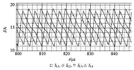
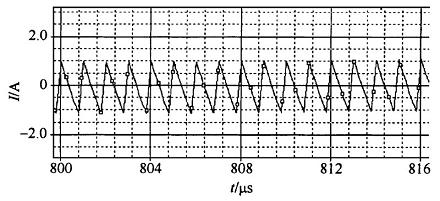
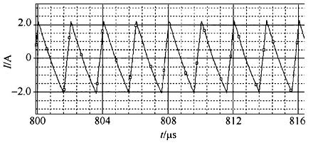
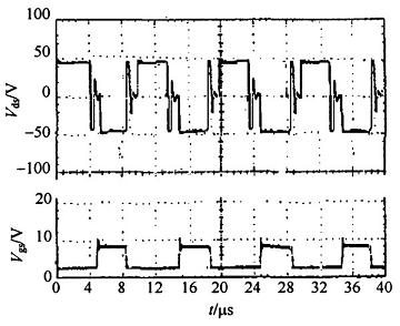
Figure 6 Waveform of filtered inductor current
Figure 7 Output current ripple waveform of interleaved parallel converter structure
Figure 8 Output current ripple waveform of single current-doubling rectifier converter structure
5 Experimental results
Through theoretical research and simulation analysis, it can be seen that the interleaved low-voltage high-current DC-DC converter has good performance, and the output current ripple can be reduced to very small when the output is 1125V/60A. In order to further illustrate the feasibility of this topology, experimental results are used to verify. The experimental circuit is shown in Figure 4. The experimental parameters are the same as the simulation. Finally, the experimental waveform shown in Figure 9 is obtained. In Figure 9, Vgs is the gate drive voltage waveform of one MOSFET at the primary side, and Vds is the gate source voltage waveform of the corresponding MOSFET. From Figure 9, it can be seen that the waveform obtained from the experimental results is very consistent with the theoretical analysis results in Figure 5, and the proposed method is feasible. Among them, the transformer uses GU22 magnetic core made of R2KB soft ferrite material, and the number of turns on the primary and secondary sides is 8 turns and 1 turn respectively; The inductor adopts the ring core T5-10-215 made of wide constant magnetic conductivity material IJ50h, with 8 turns.
Figure 8 Output current ripple waveform of single current-doubling rectifier converter structure
5 Experimental results
Through theoretical research and simulation analysis, it can be seen that the interleaved low-voltage high-current DC-DC converter has good performance. When the output is 1125V/60A, the output current ripple can be as shown in Figure 9
6 Conclusion
Through simulation and experimental analysis, the following conclusions are drawn: for low-voltage high-current DC-DC converters, the output current ripple can be further reduced by interleaving and paralleling, and the effect is very obvious; Or in the case of the same output current ripple, the filter inductance can be greatly reduced, thus reducing the size of the whole converter and improving the transient response characteristics of the converter. The case of interleaved parallel connection of two current-doubling rectifier structures discussed is also applicable to the case of interleaved parallel connection of multiple current-doubling rectifier structures.
So as to be very small. In order to further illustrate the feasibility of this topology, experimental results are used to verify. The experimental circuit is shown in Figure 4. The experimental parameters are the same as the simulation. Finally, the experimental waveform shown in Figure 9 is obtained. In Figure 9, Vgs is the gate drive voltage waveform of one MOSFET at the primary side, and Vds is the gate source voltage waveform of the corresponding MOSFET. From Figure 9, it can be seen that the waveform obtained from the experimental results is very consistent with the theoretical analysis results in Figure 5, and the proposed method is feasible. Among them, the transformer uses GU22 magnetic core made of R2KB soft ferrite material, and the number of turns on the primary and secondary sides is 8 turns and 1 turn respectively; The inductor adopts the ring core T5-10-215 made of wide constant magnetic conductivity material IJ50h, with 8 turns.
|
Disclaimer: This article is transferred from other platforms and does not represent the views and positions of this site. If there is any infringement or objection, please contact us to delete it. thank you! |


 Business consulting

 13823761625
 Mail me