Service Hotline: 13823761625

Support

Contact Us

You are here:Home >> Support >> Technology

Technology

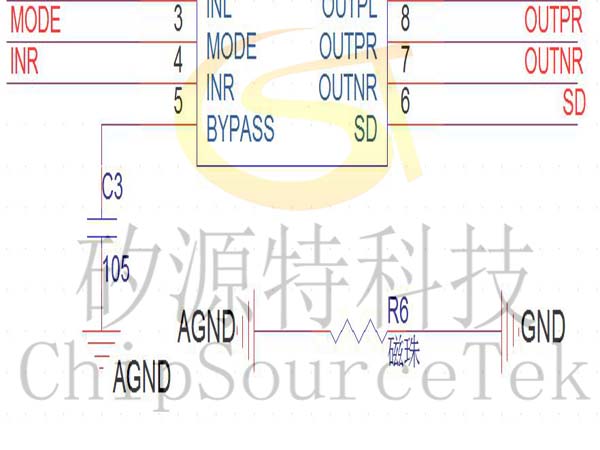
Resolution direction of power amplifier bottom noise

Time:2023-03-11 Views:1230
 Generation of bottom noise
    Generally, the bottom noise of mass produced chips is the normal value, hundreds of micro-amplitude, but in actual use, there will be various kinds of bottom noise. First, judge how the bottom noise is generated. There are three types of bottom noise:
    1、 Chip‘s own bottom noise: Generally speaking, the chip‘s own bottom noise in mass production is normal.
    2、 The bottom noise of the sound source, due to the poor processing of the board, causes the sound source itself to carry interference signals, which are transmitted to the power amplifier and output by the power amplifier, resulting in the bottom noise. (More common)
    3、 The bottom noise caused by power supply or GND, dirty power supply or fixed frequency jitter can also cause the bottom noise, which usually occurs in DC-DC. (More common), GND interference can also cause background noise

    2、 Sound source bottom noise: use the oscilloscope to test the sound source signal, and you can see whether there is too much noise, and then connect the earphone to the sound source, and listen whether the sound source has bottom noise.
    3、 Bottom noise caused by power supply or GND: use an oscilloscope to test whether the power supply is clean and whether there is a fixed frequency string in the power supply. There is a requirement for the oscilloscope bandwidth. If the GND is not clean, it will string into two places. The power ground inside the chip will cause the power supply inside the chip to be dirty, resulting in the bottom noise. In addition, if it is a single-ended input power amplifier, it will enter the reference point of the amplifier inside the chip through the BYPASS capacitor. If the reference point has interference, it will generate the bottom noise.

    Power supply and GND bottom noise: start with power supply interference, add capacitance and π type filter circuit to eliminate interference or change the frequency beyond the audio range. If GND has interference with single-ended input, BYPASS capacitance should be increased from BYPASS, or a small resistance test should be conducted in series, and then the chip audio circuit should be separated from the ground of other signals separately.
    The magnetic bead can also be used according to the actual situation. The parallel connection of resistance and capacitance should not be too large to isolate low-frequency interference. The resistance should not be too large. Generally, it is at ohm level. Too large resistance may cause jamming.


    Disclaimer: This article is transferred from other platforms and does not represent the views and positions of this site. If there is any infringement or objection, please contact us to delete it. thank you!
    矽源特科技ChipSourceTek