


Tackle the difficulties of voltage surge and current surge
Time:2023-03-22
Views:1035
In order to prevent the distributed inductance and capacitance of high-speed switching circuits in switching power supplies (switching power supplies are power supplies that use modern power electronics technology to control the time ratio of switching on and off, and maintain a stable output voltage. Switching power supplies are generally composed of pulse width modulation (PWM) control ICs and MOSFETs), which generate surge voltages and noise under the influence of accumulated charges in diodes. In this paper, an RC or LC absorption circuit is used to magnetically absorb the surge voltage generated by the accumulated charge in the diode, using an amorphous magnetic core and a rectangular magnetic core to solve the problem of generating and suppressing the surge current in the switching power supply.
introduction
The main components of switching power supplies mostly have parasitic inductance and capacitance. The parasitic capacitance Cp is generally connected in parallel with the switching element or diode, while the parasitic inductance L is usually connected in series with it. Due to the effects of these parasitic capacitances and inductances, switching elements often generate large voltage and current surges during on-off operation.
Large current surges and voltage surges occur when switching on or off and diode reverse recovery occurs. The most effective way to suppress current surges when the switch is turned on is to use a zero voltage switching circuit. On the other hand, voltage surges caused by switching off and diode reverse recovery can damage semiconductor components and also cause noise. For this reason, when the switch is turned off, an absorption circuit is required. When the diode reversely recovers, the voltage surge generation mechanism is the same as when the switch is turned off, so this absorption circuit is also suitable for diode circuits. This article introduces absorption circuits such as RC, RCD, and LC. The basic working principle of these absorption circuits is to provide a bypass for the switch when it is disconnected to absorb the energy accumulated in the parasitic inductance, and to clamp the switch voltage to suppress surge currents.
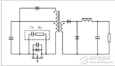
RC absorption circuit
Figure 1 RC Absorption Network Circuit
Figure 1 shows the circuit diagram of an RC absorption network. It is a circuit in which the resistor Rs and the capacitor Cs are connected in series and connected in parallel with the switch. If the switch is turned off, the energy accumulated in the parasitic inductance will charge the parasitic capacitance of the switch, as well as the absorption capacitance through the absorption resistor. In this way, due to the effect of the absorption resistance, its impedance will become larger, and the absorption capacitance will effectively increase the capacity of the parallel capacitance of the switch, thereby suppressing the voltage surge caused by the switch opening. When the switch is turned on, the absorption capacitance is discharged through the switch, and at this time, its discharge current will be limited by the absorption resistance.
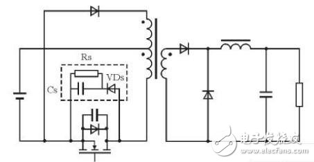
RCD absorption circuit
The RCD absorption circuit given in this article is shown in Figure 2, which consists of a resistor Rs, a capacitor Cs, and a diode VDs. The resistor Rs can also be connected in parallel with the diode VDs. If the switch is disconnected, the energy accumulated in the parasitic inductance will be charged through the parasitic capacitance of the switch, and the switch voltage will rise. When the voltage rises to the voltage of the absorption capacitor, the absorption diode turns on, causing the switching voltage to be clamped by the absorption diode (about 1 V). At the same time, the energy accumulated in the parasitic inductance also charges the absorption capacitor. During switching on, the absorbing capacitance is discharged through a resistor.
Figure 2 RCD Absorption Network
The use of RC and RCD absorption circuits can also demagnetize transformers without the need for additional demagnetization circuits consisting of transformer windings and diodes. The excitation energy of the transformer will be consumed in the absorption resistance. RC and RCD absorption circuits can not only consume the energy accumulated in the transformer leakage inductance, but also consume the transformer excitation energy. Therefore, this method also reduces the conversion efficiency of the converter.
Because the RCD absorption circuit clamps the switching voltage through a diode, the effect is better than RC. At the same time, it can also use larger resistors, but its energy loss is also smaller than RC.
LC absorption circuit
The LC circuit is a circuit composed of components such as capacitors, inductors, resistors, and electronic devices that can generate oscillating currents or have a filtering effect. The LC circuit formed by connecting the inductor coil L and the capacitor C is the simplest type of LC circuit.
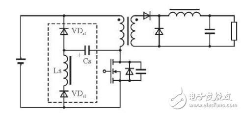
Figure 3 LC Absorption Network
The LC absorption circuit is shown in Figure 3 and consists of Ls, Cs, VDs1, and VDs2. If the switch is disconnected, the energy accumulated in inductors such as magnetic leakage or excitation can be discharged through the capacitor Cs through VDs1, causing the voltage of the absorbing capacitor Cs to reverse, thereby demagnetizing the transformer from the capacitor voltage. During this period, the polarity of the input voltage and the voltage applied to the switch by the absorbing capacitor are reversed again. Generally, the LC absorption circuit does not consume energy.
Conclusion
In order to improve the switching frequency and the quality of switching power supply products, voltage surge and current surge issues must be emphatically considered. This article proposes this effective suppression measure based on the analysis of the interference generation mechanism and a lot of practice. Therefore, to solve the surge problem, it is necessary to combine the actual design, analyze the mechanism of surge generation, and design the surge absorption circuit in combination with the actual situation to minimize the surge interference of switching power supplies.
|
Disclaimer: This article is transferred from other platforms and does not represent the views and positions of this site. If there is any infringement or objection, please contact us to delete it. thank you! |


 Business consulting

 13823761625
 Mail me