


Setting the output impedance using feedback can save 3dB of output power
Time:2023-03-28
Views:1023
Operational amplifiers are often terminated in series to match the impedance of the load. However, this practical method will generate a 3dB output power loss on the termination resistor (Figure 1). Newer operational amplifiers operate at 3V and 5V, limiting output swing, which means that series matching resistor methods should be avoided. Another method is to use a series feedback circuit to set the output impedance. John Wittman, a senior research engineer at GTE Lenkurt Electronics, introduced this technology more than 40 years ago.
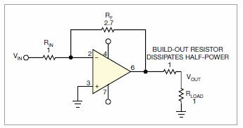
In Figure 1, using a series termination resistor that is equal to the load will waste 3dB of power, reducing the output swing by half.
With this technology, setting the output impedance can increase mutual feedback by 6 dB, achieving a return loss better than 30 dB. What needs to be added is a series current detection resistor, another operational amplifier, and a current limiting resistor (Figure 2). This example shows a high side sensor and an unbalanced load. The forward amplifier is designed to have twice the required gain at no load. In this example, the open circuit gain is 2.7 and the input impedance is 1 Ω. The input current is 1A and the input signal is 1V
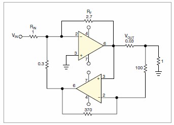
In Figure 2, this method uses a high side current detection resistor and a second amplifier to set the output impedance to match the load, thereby achieving almost all of the output swing.
To match the 1 Ω load of the amplifier, the series feedback circuit must rotate half of the input current from the negative input terminal of the operational amplifier. The original 1A input current flows through the RF?, Reducing to 0.5A means that the output voltage is half the open circuit voltage. The output impedance is now 1 Ω and the series feedback is 6 dB, so the output impedance can match the load and still achieve almost full voltage swing of the amplifier, eliminating the need to waste half of the output power on the series termination. The current detection resistance value used in this example is 3% of the output load, so the power consumption will be 3%. Through careful design, the power consumption can be reduced to less than 1%.
In telecommunication lines, in order to achieve longitudinal balance, the impedance of two conductors to ground should be equal. Longitudinal balancing prevents crosstalk and 60Hz induced noise. This is also important at the higher frequency of DSL (Digital Subscriber Line) services. Telecommunications companies generally use transformers to provide a longitudinal balance of 80 dB to 120 dB. Transformers also isolate transients caused by lightning, etc. The application of this technology can be achieved through transformer coupling and low side current detection (Figure 3). The design process is still the same, but only two resistors can provide 6dB of feedback.
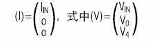
State equations can be used to formalize circuit analysis. For the circuit in Figure 2, since the negative input terminal of the operational amplifier is virtually grounded, the relationship between input voltage and current can be obtained: IIN=(VIN V -)/1 Ω=VIN/1 Ω. Due to the high impedance of the negative input terminal of the operational amplifier, the current at this terminal must be applied to 0A, thereby obtaining another equation.
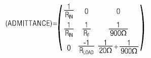
Summarize the current on V -, but the node current should refer to the detection resistance, including a resistance of 0.3 Ω and a detection resistance of 0.03 Ω: 0=VIN/1 Ω+VOUT/2.7 Ω+0.37VOUT/RLOAD. The circuit function can be expressed in vector and matrix form: (I)=(ADMITTANCE) × (V)。 It is also possible to expand the appropriate current state:


Inverse the matrix (Y) and multiply it by the matrix I, where I1 is 1A, to obtain a voltage vector for an open circuit load with a VIN equal to 1V and a VOUT of -2.7V, confirming that the design is correct.
Then, it is expanded into a vector representation of voltage:
Substitute these values into (I)=(ADMITTANCE) × (5) , Solve:
For the circuit in FIG. 2, the forcing function is I1; The input current is 1A. Inverse the admittance matrix and multiply it by the current vector to obtain the voltage vector. Using HP‘s HP-48 calculator can accomplish this difficult task. The result obtained is that the VIN is 1V, and the calculated VOUT is -1.35V, which is half of the no-load gain of 2.7. Then repeat this analysis for a load resistance of 1000 Ω:
Inverse the matrix (Y) and multiply it by the matrix I, where I1 is 1A, to obtain a voltage vector for an open circuit load with a VIN equal to 1V and a VOUT of -2.7V, confirming that the design is correct.
Be careful when writing your own equations; Two subordinate equations can easily lead to incorrect answers. The HP-48 calculator uses the "least square method" for solving problems, but it does not check for zero determinant conditions, warning you that there are dependent equations. You can use HP-48 to add up two real matrices to obtain a complex matrix. This method is convenient when your circuit model includes reactive components. If you prefer to use a computer rather than a pen and paper, you can also use Spice to analyze this circuit.
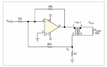
In Figure 3, you can also use the low side output current detection method to match the output impedance, and there is a transformer coupled output.
The three equations can be used to analyze the circuit in Figure 3. The input current can be expressed as a function of the input resistance: IIN=(VIN V -)/RIN=VIN/RIN. As described in the above example, the current at the negative input end of the amplifier is summed to 0: 0=VIN/RIN+VOUT/28k Ω+(V4-V -)/900 Ω, and then the current at the V4 node is added: 0=(V4-V -)/900 Ω+(V4-VOUT)/LOAD+V4/20 Ω. Express the current as a vector:
The admittance matrix becomes:
This equation determines the admittance matrix (Y).
At this point, the input current should be 100 μ A. The load resistance should be 600 Ω. Use an HP-48 calculator to inverse the admittance matrix and multiply it by the current matrix. The obtained voltage matrix can calculate that the input voltage is 1V, the output voltage is -1.4V, and V4 is -0.05V. Then, set the load to 10000 Ω. The magnetizing inductance of the transformer is assumed to be infinite. Then repeat the process to obtain an output voltage of 2.8 V
By modifying the turn ratio of the transformer, the maximum available signal power of the operational amplifier can be matched to the load. The calculated optimal output impedance of the operational amplifier signal is equal to the peak output voltage swing divided by the maximum peak capacity of the operational amplifier.
|
Disclaimer: This article is transferred from other platforms and does not represent the views and positions of this site. If there is any infringement or objection, please contact us to delete it. thank you! |


 Business consulting

 13823761625
 Mail me