


PCB Design Method for Reducing Harmonic Distortion
Time:2023-05-10
Views:961
In fact, printed circuit boards (PCBs) are composed of electrically linear materials, which means their impedance should be constant. So, why does PCB introduce nonlinearity into the signal? The answer is that the PCB layout is "spatially nonlinear" relative to where the current flows.


Whether the amplifier receives current from this power source or another power source depends on the instantaneous polarity of the signal applied to the load. The current flows out of the power supply, passes through a bypass capacitor, and enters the load through an amplifier. Then, the current returns to the ground plane from the load ground terminal (or the shield of the PCB output connector), passes through the bypass capacitor, and returns to the power source that originally provided the current.
The concept of the path with the minimum impedance through which current flows is incorrect. The amount of current in all different impedance paths is proportional to its conductivity. In a ground plane, there is often more than one low impedance path through which a large proportion of ground current flows: one path is directly connected to the bypass capacitor; The other excites the input resistor before reaching the bypass capacitor. Figure 1 illustrates these two paths. The ground return current is the real cause of the problem.
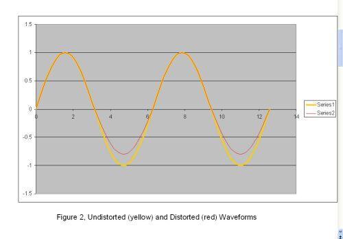
When the bypass capacitors are placed at different positions on the PCB, the ground current flows through different paths to their respective bypass capacitors, which represents the meaning of "spatial nonlinearity". If a significant portion of the component of a certain polarity of the ground current flows through the ground of the input circuit, only the component voltage of that polarity of the signal is disturbed. If the other polarity of the ground current is not disturbed, the input signal voltage changes in a nonlinear manner. When one polarity component changes while the other polarity remains unchanged, distortion occurs, manifested as second harmonic distortion of the output signal. Figure 2 shows this distortion effect in an exaggerated form.
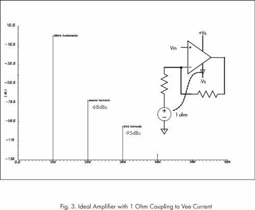
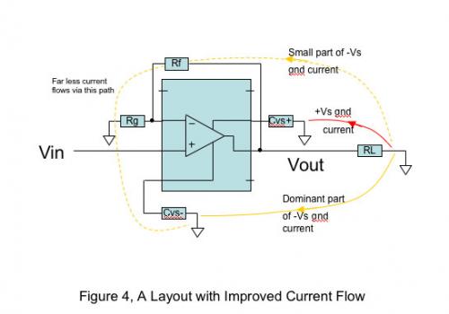
When only one polarity component of a sine wave is disturbed, the resulting waveform is no longer a sine wave. Using a 100 Ω load to simulate an ideal amplifier, where the load current passes through a 1 Ω resistor and the input ground voltage is coupled only at one polarity of the signal, the result shown in Figure 3 is obtained. The Fourier transform shows that the distorted waveform is almost entirely the second harmonic at -68dBc. When the frequency is very high, it is easy to generate this degree of coupling on the PCB, which can destroy the excellent anti distortion characteristics of the amplifier without resorting to too many special nonlinear effects of the PCB. When the output of a single operational amplifier is distorted due to the ground current path, the ground current flow can be adjusted by rearranging the bypass circuit and maintaining a distance from the input device, as shown in Figure 4.
Multi amplifier chip
The problem with multi amplifier chips (two, three, or four amplifiers) is more complex because it cannot keep the ground connection of the bypass capacitor away from all input terminals. This is even more true for four amplifiers. The four amplifier chips have input terminals on each side, so there is no space to place bypass circuits that can reduce input channel disturbances.
Figure 5 shows a simple method for four amplifier layout. Most devices are directly connected to the four amplifier pins. The ground current of one power supply can disturb the input ground voltage and ground current of another channel power supply, leading to distortion. For example, the (+Vs) bypass capacitor on channel 1 of the four amplifiers can be placed directly near its input; The (- Vs) bypass capacitor can be placed on the other side of the package. (+Vs) ground current can disturb channel 1, while (- Vs) ground current may not.
To avoid this problem, the ground current can disturb the input, but the PCB current can flow in a spatially linear manner. To achieve this goal, a bypass capacitor can be placed on the PCB in the following way: allowing (+Vs) and (- Vs) ground currents to flow through the same path. If the disturbance of positive/negative current to the input signal is equal, there will be no distortion. Therefore, arrange the two bypass capacitors closely together to share a common ground point. Because the two polarity components of the ground current come from the same point (output connector shield or load ground) and both return to the same point (common ground connection of the bypass capacitor), both positive and negative currents flow through the same path. If the input resistance of a channel is disturbed by (+Vs) current, then (- Vs) current has the same effect on it. Because the disturbance generated is the same regardless of polarity, there will be no distortion, but it will cause a small change in the gain of the channel, as shown in Figure 6.
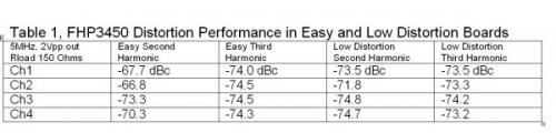
To verify the above inference, two different PCB layouts were used: simple layout (Figure 5) and low distortion layout (Figure 6). The distortion generated by the FHP3450 four operational amplifier using Fairchild Semiconductor is shown in Table 1. The typical bandwidth of the FHP3450 is 210MHz, with a slope of 1100V/us, an input bias current of 100nA, and a working current of 3.6mA per channel. From Table 1, it can be seen that the more severe the distortion, the better the improvement effect, thus making the four channels nearly equal in performance.
If there is not an ideal four amplifier on a PCB, it will be difficult to measure the effects of a single amplifier channel. Obviously, a given amplifier channel not only perturbs its own input, but also the inputs of other channels. The ground current flows through all different channel inputs and produces different effects, but is also influenced by each output, which is measurable.
Table 2 shows the harmonics measured on other channels that are not driven when only one channel is driven. The underiven channel exhibits a small signal (crosstalk) at the basic frequency, but distortion directly introduced by ground current is also generated in the absence of any significant basic signal. The low distortion layout in Figure 6 shows a significant improvement in the second harmonic and total harmonic distortion (THD) characteristics due to almost eliminating the ground current effect.
Summary of this article
Simply put, on a PCB, the ground return current flows through different bypass capacitors (used for different power sources) and the power supply itself, and its magnitude is proportional to its conductivity. The high-frequency signal current flows back to the small bypass capacitor. Low frequency current (such as the current of audio signals) may mainly flow through larger bypass capacitors. Even lower frequency currents may "ignore" the existence of all bypass capacitors and flow directly back to the power lead. The specific application will determine which current path is the most critical. Fortunately, by using a common grounding point and a ground bypass capacitor on the output side, it is easy to protect all ground current paths.
The golden rule of high-frequency PCB layout is to place the high-frequency bypass capacitor as close as possible to the power pins of the package. However, comparing Figure 5 and Figure 6, it can be seen that modifying this rule to improve distortion characteristics will not bring too much change. The improvement of distortion characteristics comes at the cost of adding approximately 0.15 inches of high-frequency bypass capacitor wiring, but this has little impact on the AC response performance of the FHP3450. PCB layout is crucial for fully utilizing the performance of a high-quality amplifier, and the issues discussed here are not limited to high-frequency amplifiers. Signals with lower frequencies such as audio have much stricter requirements for distortion. The ground current effect is smaller at low frequencies, but if the required distortion indicators are required to be improved accordingly, the ground current may still be an important issue.
|
Disclaimer: This article is transferred from other platforms and does not represent the views and positions of this site. If there is any infringement or objection, please contact us to delete it. thank you! |


 Business consulting

 13823761625
 Mail me