


Analysis of Self Inverting Circuit for BTL Audio Power Amplifier IC
Time:2023-05-23
Views:939
In BTL audio power amplifier integrated circuits, there are several methods to obtain signals of equal size and opposite phase for two sets of power amplifiers. AVL18K02200
(1) A load sharing amplification circuit using discrete electronic components to output two signals from the collector and emitter.
(2) Set up a signal attenuation circuit in the integrated circuit of BTL audio power amplifier, extract a portion of the signal from one set of power amplifier output pins, attenuate it, and add it to another set of power amplifier input pins from the inverter input end.
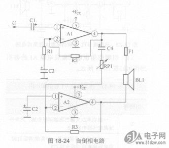
(3) The external circuit method is used for signal attenuation and phase inversion, as shown in Figure 18-24, which is a single channel BTL audio power amplifier in this form. The Al and A2 in the circuit are two single channel OTL audio power amplifier integrated circuits. Since there is no attenuation circuit in the internal circuit, an external attenuation circuit method needs to be used. BLI
Figure 18-24 Self Inverting Circuit
In the circuit, the integrated circuits Al and A2 respectively constitute two sets of amplification circuits for the BTL power amplifier. The input signal U is coupled by C1, and is fed into Al for amplification from the signal input pin ① of Al. A part of the output signal from the signal output pin ⑧ of Al is coupled by C4 and fed into the internal circuit of A2 through the variable resistor RP1 from the inverted input pin ② of A2 for amplification, and output from its ④ pin. The ④ pins of Al and A2 are the two signal output pins of this amplifier.
The signal phase of the signal output pin ④ of Al in the circuit is the same as that of the signal input pin ① of Al, while the signal phase of the inverted signal input pin ② of A2 is opposite to that of the signal output pin ④ of A2. Therefore, the signal phase of the signal output pin ④ of Al and the signal output pin ④ of A2 is opposite.
Adjusting the resistance value of the variable resistor RP1 can change the signal size of the input pin ② of the inverted signal sent to the integrated circuit A2. By adjusting the resistance value of the variable resistor RP1, the signal size of the input pin ① of the reverse signal input pin of the integrated circuit A2 is equal to that of the input pin ① of the input Al signal.
|
Disclaimer: This article is transferred from other platforms and does not represent the views and positions of this site. If there is any infringement or objection, please contact us to delete it. thank you! |


 Business consulting

 13823761625
 Mail me