


The basic architecture and working principle of LDO
Time:2023-06-07
Views:892
LDO, also known as Low Dropout Regulator, is a linear power supply that requires fewer external components for application. Some models of LDO only require a filter capacitor at the input and output terminals.

Sample the output voltage through resistors R1 and R2, compare and amplify the collected voltage with the reference voltage (expected output voltage value), and then feedback it to the input part through the PMOS gate (PNP transistor base). Dynamically stabilize the output by adjusting the transistor‘s conduction voltage drop.
Attention: ① Whether the transistor is PMOS or PNP, it must work in the linear region (amplification state). ② Due to the small conduction voltage drop of the transistor, the difference in input and output voltage can be reduced to a very small level. Therefore, the topology called low voltage difference ③ negative feedback determines that the output voltage of LDO is very stable.
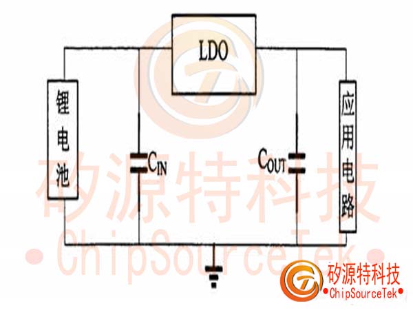
Application of LDO in Lithium Battery Chargers
As shown in the above figure, in a lithium battery charger, as the usage time of the lithium battery increases, the voltage of the lithium battery may gradually decrease, and the application circuit requires a stable power supply voltage, such as 2.5V. In this way, only one LDO needs to be added between the lithium battery and the application circuit. When the input voltage of the LDO is within the range of operating voltage changes, the output voltage of the LDO is stable (2.5V), At this point, the application circuit can be powered by the output voltage of the LDO. LDO has a wide range of applications, but there are still many technical shortcomings in current LDO, such as high Dropout voltage, high static current, low conversion efficiency, and low output current. In order to make up for the shortcomings of these technical indicators, LDO is developing in the following directions: (1) Dropout voltage is getting lower and lower; (2) The static current is decreasing; (3) The output current is increasing; (4) The output noise is decreasing; (5) The quantity required for capacitors is decreasing; (6) The additional functions are becoming more and more complete; (7) The packaging area is getting smaller and smaller; The direction of high current output is an important direction for the development of LDO. Therefore, this article mainly studies the direction of high current and high stability of LDO.
The basic architecture and working principle of LDO
LDO is a DC buck linear regulator that can maintain stable output voltage even when the input voltage or load current changes.
Nowadays, LDO circuits have the characteristics of small size, low noise, low power consumption, low price, and convenient use. However, their basic structure is relatively simple, including four modules: voltage reference source (VREF), error amplifier (EA), adjustment transistor (MPASS), and feedback resistor (Rl, R2), as shown in the following figure. Among them:
The voltage reference source provides a high-precision reference voltage for the error amplifier. The error amplifier, adjustment tube, and feedback resistor form the control loop of the LDO. When the input voltage or load current changes, the output voltage VoUT also needs to make corresponding changes. At this time, the LDO can suppress the changes in the output voltage Votrr through its negative feedback regulation effect of the control loop.
As shown in the figure, when the output voltage decreases, the feedback voltage VFB also decreases correspondingly through the voltage sharing effect of the feedback resistors R1 and R2. The reference voltage is provided by the reverse input terminal of the error amplifier, which provides a stable reference voltage. The feedback voltage VFB is connected to the forward input terminal of the error amplifier, and the output voltage VEA of the error amplifier decreases accordingly.
After that, the gate voltage of the regulating tube MPASS decreases, the difference between the gate source voltage increases, the drain current increases, and the output voltage Votrr increases accordingly, which suppresses the decrease of the output voltage Votrr, thus maintaining a stable output.
The error amplifier is used to compare the output feedback sampling signal with the reference voltage, and after amplifying the difference signal, it is output to the gate of the adjustment tube to control the working state of the adjustment tube and maintain a stable output voltage. It can be regarded as a transconductance amplifier in LDO linear regulators, along with the adjustment transistor, and its transconductance directly affects the voltage regulation rate and load regulation rate characteristics of the regulator. Reducing the voltage regulation rate and load regulation rate requires increasing the transconductance, which will inevitably increase the bias current in the circuit.
However, it is also necessary to meet the requirement of low static current flow: the output impedance of LDO regulators is relatively high, which is greatly affected by the load and can easily cause system instability. Usually, the equivalent series impedance (ESR) of the output capacitor is used for frequency compensation to improve its stability. The error amplification circuit obtains the feedback voltage Vfb proportional to the output voltage Vout through the sampling resistance, compares Vfb with the reference voltage Vref, and outputs an error amplification signal Vdrive, thereby controlling the grid potential of the adjusting tube M1 (PMOS tube), realizing the adjustment of the output current of M1, so that Vout is stable; At the same time, the stability of the voltage regulator is ensured by using dynamic zero frequency compensation. In deep negative feedback, the output voltage of the LDO linear regulator only depends on the resistance ratio and reference voltage (VREr) of the control loop, and is not related to the size of other parameters such as input voltage and load current. Under a certain range of power supply voltage, to increase the output voltage of the LDO, it is necessary to reduce the feedback coefficient (F) or increase the reference voltage (VREF), which needs to be determined based on the actual output voltage requirements of the circuit.
|
Disclaimer: This article is transferred from other platforms and does not represent the views and positions of this site. If there is any infringement or objection, please contact us to delete it. thank you! |


 Business consulting

 13823761625
 Mail me