


Layout considerations for synchronous step-down converters
Time:2023-08-04
Views:692
The buck DC/DC converter (see Figure 1) is a very popular switch DC/DC voltage regulator topology, widely used in many electrical and electronic applications, from cloud infrastructure to personal electronic products, to factory and building automation. They account for over 75% of all non isolating switch voltage regulator topologies today.

The layout of the buck converter is as important as simulation and design, but the lack of good layout practices may delay development time and even cause operational and reliability issues.
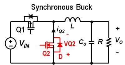
Synchronous depressurization
Figure 1: Synchronous buck DC/DC converter
The factors considered for layout include bypass capacitors, feedback compensation network components, power components, parasitic components, grounding circuits, and connections.
Bypass capacitor
For bypass capacitors, minimizing lead inductance is important and can be achieved by reducing the bypass circuit area, shortening the length of high di/dt (current conversion rate) paths, using grounding layers as much as possible (if possible), introducing current paths at both ends of the capacitor, and avoiding multiple layouts. In addition, it is important to connect different types of capacitors in parallel to reduce the impedance at both ends of the capacitor frequency band, as it can reduce the frequency range from 2MHz to 20MHz (typical capacitor values are 0.1 μ F to 0.01 μ F) The impedance decreases. Traction capacitors bring them closer to the pins of integrated circuits (ICs) and can also display key nodes and areas to layout designers, as shown in Figure 2.
Figure 2: Bypass capacitor circuit connection indicating critical loop area
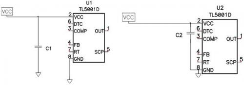
Feedback compensation network
Place the compensation network near the IC error amplifier. Place resistors so that they are directly connected to the inverting input of the error amplifier (FB pin), as shown in Figure 3.
Figure 3: Feedback Compensation Network Layout
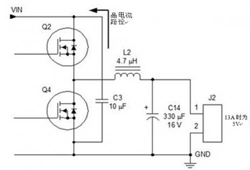
Power component
Ensure the correct connection of the power component, as there is a high di/dt (current conversion rate) in the current path, as shown in Figure 4. Any inductance in the path will cause the switching node to ring, which may exceed the absolute maximum rating of the power FET, and will also generate harmonics and unnecessary noise in the system. The goal is to minimize the circuit area by using an assembly of double-sided printed circuit boards (PCBs), with MOSFETs (metal oxide semiconductor field-effect transistors) on one side of the PCB and capacitors on the other side. Ensure correct placement and deployment of components. Correct design does not require buffering circuits to reduce switching node ringing.
Figure 4: Power component connection indicating high current path
parasitic component
Pay attention to parasitic components as they may introduce and increase impedance in the power supply, which can lead to stability and operational issues. Pay attention to the wiring inductance, especially for low impedance circuits and filters, power switches, and timing circuits. Use a ground plane and wide wiring to minimize inductance. In terms of circuit board capacitance, pay attention to high impedance or noise sensitive circuits, and pay attention to the coupling between circuit board planes/layers and component pads. Magnetic coupling may also occur between inductors, especially annular inductors. In this case, please consider other installation directions. Magnetic coupling may also occur between loops, therefore, the loop area should be minimized and a grounding plane should be used.
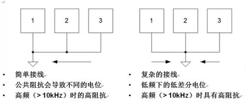
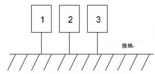
Grounding circuit and connection
There is a problem of series or parallel connection with single point grounding, as shown in Figure 5.
Figure 5: Series and parallel single point grounding connection
A better method is to use multiple grounding points. As shown in Figure 6, multi-point grounding allows for low impedance between circuits to minimize potential differences and also reduces circuit wiring inductance. The purpose is to include high-frequency current in a single circuit and maintain it outside the grounding plane.
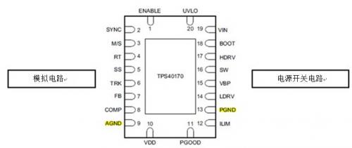
Many buck converters control ICs to recognize noise and quiet circuit areas, and the arrangement of IC pins makes it easier to layout and component placement around the IC pins. Some even provide separate pins for power supply and analog grounding, such as the TPS40170 60V synchronous buck pulse width modulation (PWM) controller pin shown in Figure 7.
Figure 7: IC pins of the buck controller for analog and power connection
Therefore, layout planning around the IC pin layout and using the layout practices mentioned in this article can help you obtain the correct buck converter design from the beginning and avoid any future troubles.
|
Disclaimer: This article is transferred from other platforms and does not represent the views and positions of this site. If there is any infringement or objection, please contact us to delete it. thank you! |


 Business consulting

 13823761625
 Mail me