


Introduction to Boost Converter,Structure and Design
Time:2023-10-19
Views:512
Boost converter power stage
As the names‘ boost ‘and‘ boost ‘imply, the topology we are discussing today can achieve an output voltage higher than the input voltage. This, along with the improvement in efficiency, represents the key advantage of switching mode over linear regulation, as the latter cannot produce V OUT higher than V IN.
However, using switch mode technology, all we need is a different arrangement of the same simple components used for the buck converter. Figure 1 shows the appearance of this boosting arrangement.
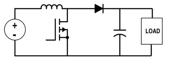
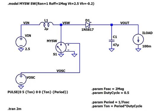

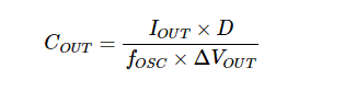
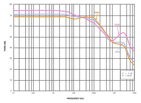
Figure 1. Circuit diagram of the boost voltage regulator. Image provided by Robert Kem
Now I will create a boost converter design for LTspice. Like the LTspice buck converter, I will use voltage controlled switches instead of transistors.
My implementation is shown in Figure 2: it represents a circuit for low voltage, battery powered applications, and the value I have chosen reflects this. I will elaborate on this in the next section.
Figure 2. Schematic diagram of a boost converter implemented in LTspice. Image provided by Robert Kem
Is it a boost regulator or a boost converter? What is a switching regulator? Review terminology and basic concepts.
Working parameters and component values
Before running the simulation based on this schematic, let‘s consider the parameters of the boost converter.
Input and output voltage
The 2.5V power supply of the boost converter provides input voltage, which we can obtain from a pair of partially discharged alkaline button batteries. However, like other switches, the complete circuit (i.e. combining the power stage with a feedback system for output voltage regulation) will be compatible with a range of input voltages. Therefore, the same circuit can be combined with a 3V lithium-ion button battery or a single alkaline battery.
The specified output voltage is 5 V. I can imagine a device where the 5 V directly supplies power to some higher power drive circuits and connected sensor or relay modules, and the 5 V is then used through one or more compact linear regulators to achieve lower voltage power digital circuits and high-precision analog circuits. I like this power management solution: although the battery voltage gradually decreases, it provides us with a stable 5 V power rail that can directly or indirectly reliably power all components in the system.
Duty cycle
The ideal relationship between the input voltage, output voltage, and duty cycle of the boost regulator is as follows:
Our V IN=2.5 V and V OUT=5 V. Since I will not intentionally incorporate non ideal factors into the simulation, I will keep the efficiency at 100%. This provides us with a 50% duty cycle.
For those who have not yet read the previous article, I would like to emphasize that we cannot rely on a fixed duty cycle to generate the required output voltage. The above equation provides us with a starting point, but in practical implementation, we will rely on closed-loop control to adjust the duty cycle as needed to maintain an appropriate V OUT.
inductance
I used a formula to determine the original inductance value of the LTspice step-down converter. However, when I tried to use the same method for the boost converter, my second attempt generated an inductance value that was one order of magnitude larger than what I hoped to use in compact low-voltage equipment.
Fortunately, this calculated inductance is not necessary for successful converter operation: instead of looking for a different formula, I chose a value that meets my suggested size limit and used it. The 2 shown in Figure 2 μ The H inductance is based on the recommendations for the boost converter inductance in the Texas Instruments (TI) application notes, which also includes the formula I initially used and other useful information about inductor selection.
switching frequency
Because I chose a relatively small inductance, I also chose a higher switching frequency. This is one of the basic relationships in the design of switching regulators: higher switching frequency can achieve lower inductance. My f OSC is 2 MHz, which is quite high for the switch, but it is not unrealistic.
Output capacitance
You can use the following formula to calculate the expected output current (I OUT), duty cycle (D), switching frequency (f OSC), and required output ripple based on( Δ V OUT) Calculate satisfactory output capacitance:
However, based on the application characteristics I described above, there is no special need to maintain low ripple. As I suggested earlier in this article, this circuit can also be connected to a linear regulator, in which case it will benefit from the ripple suppression function of the linear regulator.
I finally decided to skip the calculation. Like inductance, I used advice from real-world integrated circuits to come up with a value that I believe is a good compromise between performance and size.
Linear voltage regulator PSRR
When discussing this topic, the ripple suppression capability of linear regulators is measured using PSRR (Power Supply Rejection Ratio)?? Measurement. PSRR fluctuates based on multiple parameters, including frequency; The following figure (Figure 3) shows this fluctuation.
Figure 3. Relationship between PSRR and ripple frequency. Image provided by Texas Instruments (TI)
A chart of PSRR (in decibels) relative to ripple frequency (in hertz). It indicates that once the frequency exceeds the 10k Hz threshold, PSRR will decrease and become less stable.
Although we still have a significant attenuation at 2 MHz, if you plan to use a linear regulator to reduce the output ripple amplitude, this figure provides evidence to support the selection of a lower switching frequency.
Diode reverse recovery time
We have another parameter to discuss: the reverse recovery time of the converter diode, which is particularly important for switching regulators (if you are interested in learning more, this article on selecting the correct rectifier for your power circuit is a great resource).
Although I used standard diodes in the buck converter, I chose Schottky diodes in the boost converter. Schottky diodes are usually used as switching regulators because they can more effectively switch between conduction and non conduction states, and have lower voltage drop when conducting.
|
Disclaimer: This article is transferred from other platforms and does not represent the views and positions of this site. If there is any infringement or objection, please contact us to delete it. thank you! |


 Business consulting

 13823761625
 Mail me