


Key Points for PCB Design of High Current Power Circuits
Time:2023-10-28
Views:529
In our conventional understanding and learning, most people may say that analog signals are continuous small signals, such as sound signals. In fact, there is another type of analog signal that we need to pay attention to, which is when designing PCB in high current power circuits. Typical applications are power sources, motors, and other current converters, or situations with high current loads.
Point 1: What kind of signal is processed as a power signal?
Generally, power signals are relative to digital signals and analog small signals. For example, commonly used digital devices are logic chips, MCU chips, 232 transceiver chips, ADC chips, etc. These types of power consumption are relatively low, and during design, conventional wiring can basically meet their current consumption. Power circuits are all current paths with relatively high currents, and there are no fixed requirements. They are a relative concept that usually requires hardware engineers to evaluate and provide a reference. Personally, I am accustomed to categorizing signals with 0.5-1A, and refer to the power path for simple processing. If the current is greater than 1A, it is processed according to the power signal. The larger the current exceeds 1A, the more factors need to be considered and the more processing methods need to be used.
Key point 2: What should be paid attention to when wiring high current and power signals? How to handle it?
Firstly, due to the presence of large currents, there may be disturbances when the power ground flows through them. Secondly, during the variation of large currents, it is easy to generate EMC interference radiation. Therefore, when designing high current PCBs, the following points should be noted:
(1) Try to separate the layout of digital devices for high current paths and small signals to avoid mutual interference.
(2) When wiring a PCB, try not to cross wire the high current path and digital signals to avoid mutual interference. Especially when simulating the acquisition of signals such as ADC, it is necessary to stay as far away from the path range of high currents as possible.
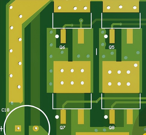
(3) The high current path should be treated with solid copper as much as possible. Firstly, the current carrying capacity is relatively high, secondly, it will have good heat dissipation effect, and thirdly, it is necessary to avoid high impedance of the wiring and large voltage drop on the wiring.
(4) Pay attention to the heat generated by high currents. The accumulation of heat can cause device damage and product damage. The power path of high currents should be particularly careful. Generally, a large area of copper is laid (copper is a good thermal conductor), and more holes are drilled (try to connect copper or heat dissipation pads, the larger the hole, the better the heat dissipation, but do not use mechanical holes). The external impedance welding layer should be excavated to expose the copper directly, Use heat dissipation fins and other methods in PCB design to accelerate heat dissipation.
(5) In the layout, consideration should be given to the issue of EMC radiation from high currents, and attention should be paid to isolating and shielding the surrounding radiation during the process of high current switching. Therefore, the high current path should be as short as possible, and the path should be carefully planned and placed away from easily interfering devices (signal interference and thermal effects).
|
Disclaimer: This article is transferred from other platforms and does not represent the views and positions of this site. If there is any infringement or objection, please contact us to delete it. thank you! |


 Business consulting

 13823761625
 Mail me