


Design a current mode controlled step-down converter in LTspice
Time:2023-12-19
Views:361
Current Mode Control (CMC) has been theoretically summarized as a technology for achieving high-performance voltage regulation in DC-DC converters. Now we will use LTspice to carefully study the actual working principles of these circuits.
I have created an LTspice schematic diagram (Figure 1) for the CMC buck converter to help us examine the design principles and operation of the CMC. This circuit is a closed-loop system that uses voltage and current feedback to lock the output voltage.
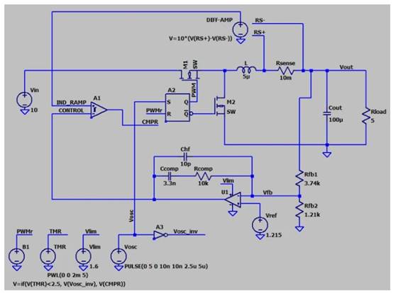
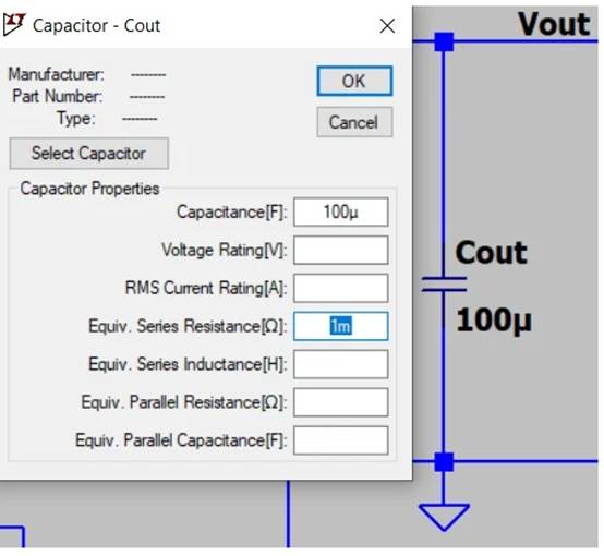
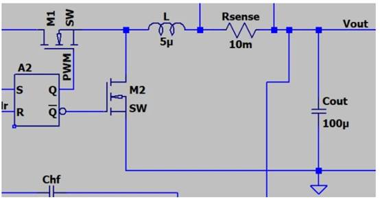
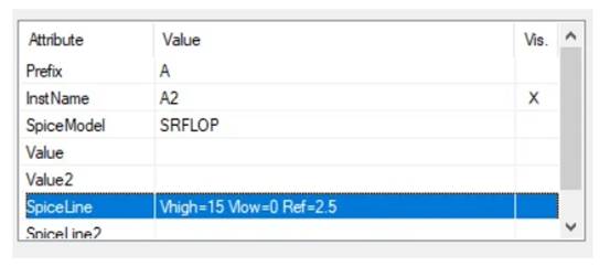
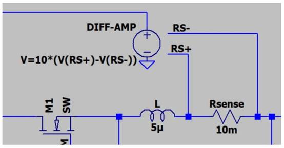
Figure 1. LTspice schematic diagram of peak CMC buck converter.
Schematic review
This implementation is based on the peak CMC buck converter shown in Figure 6 of the Texas Instruments (TI) document "Understanding and Applying Current Mode Control Theory.". There are some important differences that I will explain when relevant. Now, let‘s examine the components of this schematic and how they contribute to the functionality of the circuit.
R Sense and DIFF-AMP
Generate a current feedback signal by amplifying the voltage at both ends of the current detection resistor (R SENSE) connected in series with the inductor (L). For convenience, I use any behavioral voltage source (DIFF-AMP) instead of the SPICE version of the differential amplifier. The DIFF-AMP output is equal to the voltage at both ends of R SENSE multiplied by 10.
The total current and voltage gain can be calculated as follows: RSENSE × GDIFF? AMP=10 m Ω × 10 V/V=0.1 V/A
Feedback voltage and error amplifier
The output voltage is connected to a resistive voltage divider composed of R FB1 and R FB2. This voltage divider transmits feedback voltage (V FB) to a compensating error amplifier composed of V REF, U1, R COMP, C COMP, and CH HF.
Complete control loop
A1 and A2 complete the control loop by using current feedback signals and voltage error signals to generate appropriate gate drive waveforms for the switch. In this schematic, the switch is implemented as an NMOS transistor. A1 is a Schmitt trigger buffer that serves as a comparator due to its differential input, while A2 is an SR latch. LTspice refers to it as SRFLOP.
Power level
M1, M2, L, R SENSE, and C OUT belong to the power level. Please note that the C OUT value (Figure 2) includes an ESR of 1 m Ω.
The LTspice window displays the simulated output capacitance value of the CMC buck converter. The capacitance is 100 F and contains 1 m Ω ESR.
Figure 2 Simulated C OUT of CMC buck converter (including ESR).
I have already discussed the buck topology in previous articles, so I won‘t spend too much time here. However, I would like to comment on certain aspects of the power stage of this specific circuit, namely the gate driving voltage of M1 and the presence of two switches (rather than switches and diodes). We will discuss these in the next two sections.
M1 and M2 can be seen on the left side of Figure 3, which shows the power stage of the step-down converter.
Part of the LTspice schematic. The complete schematic shows the CMC buck converter. This schematic shows the power stage of the step-down converter.
Figure 3. Power stage section of the schematic diagram of the CMC step-down converter in Figure 1.
Boost M1 gate drive
As I mentioned earlier, we use NMOS transistors as power switches (M1). We cannot drive the gate with any old logic signals like the source of FET is grounded.
The main logic voltage in this circuit is 5V. Since V OUT is also 5V, we can easily conclude that a gate voltage of 5V is not sufficient to convert the FET into an effective switch. Anyway, we hope the gate voltage is higher than V IN, not just V OUT.
The physical implementation can solve this complex problem by incorporating a charge pump circuit to enhance the gate drive signal. The solution is simpler through LTspice implementation: I only need to tell the SR latch to use 15V as the logic high voltage (Figure 4).
The LTspice window displays the SRFLOP value. It displays a logic high voltage equal to 15 V and a logic low voltage equal to 0 V.
Figure 4 The logic high voltage definition of SR latch (SRFLOP).
Synchronous rectification
The technology of using switches instead of diodes is called synchronous rectification. This method has a series of advantages: citing TI‘s application explanation on synchronous rectification in power converter design, it "improves efficiency, thermal performance, power density, manufacturability, and reliability, and reduces overall system costs" in power supply systems
With such recognition, it is difficult to defend my use of diodes in switch simulations. Due to the fact that driving a FET to complete conduction reduces the voltage smaller than a forward bias diode, synchronous rectification is more desirable in practical applications. However, when the goal is to explain the basic principles rather than optimize performance, diodes do appear simpler. On the other hand, perhaps I just miss circuit design before the 1990s.
Anyway, the second switch must have its own driving signal, because when the high side FET (M1) conducts current, the low side FET (M2 in the schematic) needs to block the current, and vice versa. I usually find this requirement a bit annoying, but in this case, there is no problem at all - we have already used an SR latch to generate a PWM signal, and the Q-not output of the latch is exactly what our second FET needs.
Measure current
Switching regulators are known for their ability to convert voltage through power consumption, but it is somewhat disappointing that we must place resistive components in potential high current circuit paths (Figure 5). But overall, in order to gain the benefits of current mode control, this is only a small cost.
Part of the LTspice schematic. The complete schematic shows the CMC buck converter. This schematic diagram shows the current detection resistance.
Figure 5. Current detection resistance (R SENSE).
The value of R SENSE (10 m Ω) is an attempt to balance efficiency and accuracy - we aim to reduce power consumption while generating a sufficiently large voltage to compete well with noise and amplifier non ideal situations. My amplifier is a purely mathematical component, and unless you intentionally include it, the SPICE circuit will not have noise, so if we are willing, we can use smaller resistors in this simulation.
In physical circuits, devices like INA240 are a good choice for amplifying R SENSE voltage.
|
Disclaimer: This article is transferred from other platforms and does not represent the views and positions of this site. If there is any infringement or objection, please contact us to delete it. thank you! |


 Business consulting

 13823761625
 Mail me