


How to meet EMI test requirements without inductors
Time:2024-01-15
Views:286
Author:
Tony Armstrong
Marketing Director of power products of linglilte company
introduction
A basic principle for switching power supply is that it must not produce a lot of noise. Therefore, a quiet, well regulated power supply is important for achieving optimal performance in many circuit applications. In order to achieve this level of performance, it is critical to be able to reduce any noise generated during the conversion process. An obvious way to achieve this goal is to use a linear regulator. However, although linear regulators can provide quiet power rails, their conversion efficiency is not good at high step-down ratio, which will lead to thermal problems in design in high output current applications.
Of course, switching regulators based on magnetic components can alleviate common thermal problems, because they usually have high conversion efficiency, which can simplify the thermal design when the final application requires high output current. As we all know, component selection and circuit board layout will play an important role in determining the success or failure of almost all power supply designs. These aspects set their functional EMI and thermal operation mode. For novices, switching power supply layout may look like a "black" art, but in fact it is a basic part of design, which is often ignored in the early stage of the design process. Since functional EMI requirements must always be met, what is beneficial to the functional stability of the power supply is often beneficial to its EMI radiation index. In addition, a good layout from the beginning will not add any cost to the design, and it can actually save costs by eliminating the need to add EMI filters, structural shielding, EMI test time and many circuit board modifications.
Moreover, when multiple dc/dc switching mode regulators are used in the design to generate multiple power rails, or current sharing and high output power are achieved through the parallel connection of regulators, the potential interference problems caused by noise will be aggravated. If all operate at a similar frequency (switching operation), the combined energy generated by multiple regulators in a circuit will be concentrated at one frequency. The existence of this energy will become a problem, especially if the remaining ICs on the printed circuit board (PCB) and other system boards are close to each other and are vulnerable to the adverse effects of this radiation energy. This can be particularly troublesome in industrial and automotive systems with high installation density and usually close to electrical noise sources (such as mechanical switch inductive loads, PWM drive power outputs, microprocessor clocks, and contact switches). In addition, if switching operations are performed at different frequencies, intermodulation components will be mixed into sensitive frequency bands.
Switching regulator radiation
In the situation of low heat dissipation and high efficiency, switching regulator is often used to replace linear regulator. Moreover, switching regulator is usually the first active component on the input power bus line, which has a significant impact on the EMI performance of the whole product design.
Conducted radiation "rides" on the wires and wiring connected to a product. Since the noise is concentrated on a specific terminal or connector in the design, compliance with the conducted radiation requirements can usually be ensured early in the development process by using good layout or filter design. Radiation emission is a completely different thing. Each component and circuit that transmits current on the circuit board radiates an electromagnetic field. Each wire on the circuit board is an antenna, and each copper plane is a resonator. Any electrical signal (except pure sine wave or DC voltage) will generate noise in the whole signal spectrum. Even with careful design, the power designer will never really know how bad the radiation emission will be before testing the system. Moreover, the radiation emission test can not be formally implemented until the design is basically completed.
Filters are often used to reduce EMI by attenuating the signal strength at a specific frequency or within a frequency range. Part of the energy (radiation energy) transmitted through space is attenuated by adding metal and magnetic shielding. The part of energy (conducted energy) that "rides" on the PCB routing line is suppressed by adding ferrite beads and other filters. Although EMI cannot be eliminated, it can be attenuated to an acceptable level for other communication, signal processing and digital components. In addition, several regulatory agencies enforce standards to ensure compliance in both industrial and automotive systems.
The new input filter module using surface mount technology has better performance than the through-hole component. However, the pace of improvement lags behind the growth of demand for high-frequency switching regulators. Due to the fast switching, the low minimum on-off time required at higher operating frequency will produce higher harmonic components, which will increase the radiated noise. However, these high switching edge rates are necessary to achieve high conversion efficiency. The switched capacitor charging pump does not operate in this way, because it operates at a much lower switching frequency, and the most important thing is that it can allow slow switching, without causing efficiency reduction.
The smart and knowledgeable PCB designer will reduce the thermal circuit and adopt the shielding ground plane as close as possible to the active layer. However, the configuration of the device pins, the packaging structure, the thermal design requirements and the packaging size required to store sufficient energy in the decoupled components determine that the thermal loop size must be minimized. What makes things more complicated is that in a typical planar printed circuit board, the magnetic or transformer type coupling between wires higher than 30MHz will weaken the various functions of the filter, because the higher the harmonic frequency, the stronger the harmful magnetic coupling.
Switched capacitor charging pump
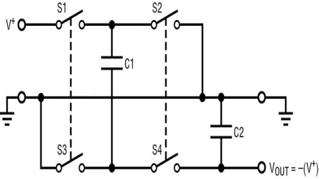
Charging pumps have existed for decades. They provide dc/dc voltage conversion and use a switching network to charge and discharge two or more capacitors. The basic charging pump switching network switches between the charging and discharging states of the capacitor. As shown in Figure 1, "flying capacitor" C1 is responsible for transporting charge back and forth, and "energy storage capacitor" C2 is used to store charge and filter output voltage. Additional "flying capacitor" and switch array can achieve a variety of gains.
Figure 1: simplified charging pump block diagram of voltage inverter
When the switches S1 and S3 are on (i.e. closed), while the switches S2 and S4 are off (i.e. open), the input power supply is charged for C1. In the next cycle, S1 and S3 are disconnected, S2 and S4 are turned on, and the charge is transferred to C2, resulting in Vout=– (v+).
However, until recently, the charging pump has the problem of limited input and output voltage range, which limits its use in industrial and automotive applications where the input is often as high as 40V or higher.
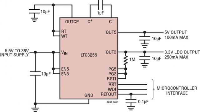
The latest product launched in this field is the ltc3256 of linglilte. It is a dual output power supply with high integration, high voltage and low noise. It uses a single positive input voltage without inductors and provides 5V and 3.3V step-down power supplies with high efficiency. The device operates in a wide range of 5.5V to 38V input voltage, including dual outputs that can be independently enabled: a 5V 100mA power supply and a 250mA 3.3V Low Dropout (LDO) regulator, providing a total of 350mA available output current. Compared with the dual LDO solution, the power consumption of these regulators combined will be much lower. For example, when the 12V input and two outputs are the maximum load, the power consumption of the ltc3256 is reduced by more than 2W (compared with the dual LDO scheme), which significantly reduces the heat loss and input current. The complete schematic diagram of this device is shown in Figure 2.
Figure 2: schematic diagram of ltc3256 with one 5v/100ma output and one 3.3v/250ma output
Ltc3256 is specially designed for systems that meet the requirements of iso26262 diagnostic coverage, and incorporates rich safety and system monitoring functions. The device is very suitable for various applications that require high voltage input to provide low noise and low power rail, such as Automotive ECU/can transceiver power supply, industrial/Telecom housekeeping power supply, and universal low power conversion.
By running the charging pump in the 2:1 mode, the ltc3256 maximizes efficiency within the widest possible working range, and automatically switches to the 1:1 mode when necessary to keep consistent with VIN and load conditions. Controlled input current and soft switching minimize conducted and radiated EMI. When both outputs are in the regulated state (no load), the quiescent current of the device is only 20 μ A. 1 in shutdown mode μ A. The integrated watchdog timer, independent power good output and reset input ensure reliable system operation and fault monitoring. The 1.1V buffered reference output allows system self-test diagnostics for applications critical to safe operation. The ltc3256 also provides additional safety features, including overcurrent fault protection, overheating protection, and 38V input transient tolerance.
The graph in Figure 3 below highlights the excellent power consumption characteristics of the ltc3256. At 12vin, the ltc3256 with 3.3v/250ma and 5v/100ma outputs consumes about 750mW, while the power consumption of the dual LDO scheme under the same conditions is almost 3W. In other words, the power consumption of the ltc3256 is 2.25w less, which is a huge benefit for the thermal aspect of the design.
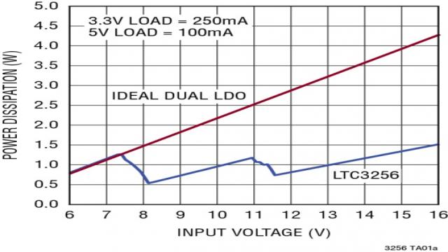
Figure 3: comparison of power consumption characteristics between ltc3256 and dual LDO
conclusion
As we all know, EMI considerations need to be carefully considered during the initial design process to ensure that they will successfully pass EMI tests when the system design is completed. So far, except for very low-power systems, there is no foolproof way to ensure that the right power IC selection can be easily achieved. However, with the recent introduction of low EMI regulators such as the ltc3256 high voltage charging pump, there is now an alternative available. It can provide much higher efficiency and lower power consumption (when compared with linear regulators), and does not have to deal with the compensation, layout, magnetism and EMI problems when using switching regulators.
|
Disclaimer: This article is transferred from other platforms and does not represent the views and positions of this site. If there is any infringement or objection, please contact us to delete it. thank you! |


 Business consulting

 13823761625
 Mail me