


Four types of MOSFETs
Time:2024-01-20
Views:271
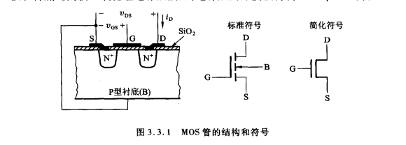
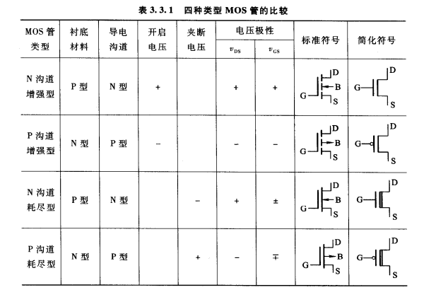
The channel, i.e. MOS transistor, is an enhanced type. The arrow on substrate B points towards the interior of the MOS transistor, indicating that the conductive channel is N-type. The gate lead out end is drawn on the side near the source electrode.
2. P-channel enhanced type
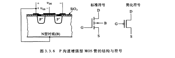
The symbol of P-channel enhanced MOSFET is shown in Figure 3.3.6, where the arrow pointing outward on the substrate indicates that the conductive channel is P-type.

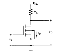
When v=0, the MOSFET is not conducting and the output is at a low level. VoL. As long as R is much smaller than the cutoff internal resistance of the MOS transistor RorF, then. VoL=VvD.
When v1
1. N-channel depletion type
The structural form of N-channel depleted MOSFETs is the same as that of N-channel enhanced MOSFETs, both using P-type substrates and N-type conductive channels. The difference is that in the depletion of VpD type MOSFETs, a certain concentration of positive ions is doped into the silicon dioxide insulation layer below the gate. The electric field formed by these positive ions is sufficient to attract a few charge carriers - electrons - from the substrate to the substrate surface below the gate, forming conductive channels between D-S. Due to this, conductive channels already exist when vCS=0. VC3 increases; When it is negative, the conductive channel v becomes wider when it is positive, and i vGS becomes narrower and i decreases.
Until v is less than a certain negative voltage value VcS (eff), the conductive channel disappears and the MOS transistor cuts off. Figure 3.3.8 of V6S (eff) shows the pinch off voltage of an N-channel depletion MOSFET with P-channel enhancement. The switch circuit diagram 3.3.9 of MOS transistor connection is the symbol of N-channel depletion type MOS transistor. In the diagram, D-S is connected, indicating the presence of conductive channels when vCS=0. The rest of the drawing is the same as the enhanced MOSFET. During normal operation, the substrate of N-channel depleted MOSFETs should also be connected to the potential of the source or system.
2. P-channel depletion type
The structure of P-channel depletion type MOSFETs is the same as that of P-channel enhancement type MOSFETs, and they are also N-type substrates with P-type conductive channels. The difference is that in P-channel depletion type MOSFETs, when vcs=0, conductive channels already exist in vCs. When the VCS is negative, the conductive channel is further widened and the value of i increases; When vCS is positive, the conductive channel narrows and i decreases. When the positive voltage of (v) is greater than the clamping voltage Vcs (odf), the conductive channel disappears and the tube cuts off.
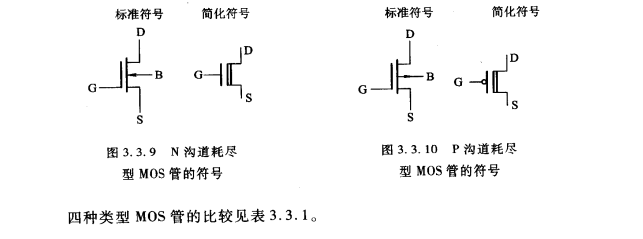
Figure 3.3.10 is the symbol of a P-channel depletion MOSFET. When working, its substrate should be connected to the source electrode, or the substrate should be connected to the potential of the system.
|
Disclaimer: This article is transferred from other platforms and does not represent the views and positions of this site. If there is any infringement or objection, please contact us to delete it. thank you! |


 Business consulting

 13823761625
 Mail me