


Design of D class amplifier based on GaN
Time:2024-01-22
Views:266
High fidelity sound reproduction enthusiasts are the latest beneficiaries of the basic quality of gallium nitride (GaN), as it allows them to breathe in challenging environments. GaN has solved their challenge regarding the optimal composition of home audio settings.
The basic categories of audio amplifiers are Class A, Class AB, and Class B, which utilize the linear region of their transistors while attempting to reconstruct a perfect input audio signal with minimal distortion. It has been shown that this design can achieve up to 80% theoretical efficiency, but in reality, their efficiency is about 65% or lower. In today‘s battery powered smartphones, digital enhanced wireless technology (DECT) smartphones, and Bluetooth speakers, this linear method has become a thing of the past because it has a huge impact on battery life. Like most other fields in the electronics industry, enthusiasts have found that using switching methods provides better commitment than linear methods.
For users who insist on using classic amplifier topology categories, their requirements will focus on accurate audio reproduction, with little consideration given to the overall electrical efficiency of the solution. Although this is entirely reasonable in home audio environments, many applications require high amplifier efficiency. This may be to save energy and extend battery life, or to reduce heat dissipation, making the final product denser and more compact.
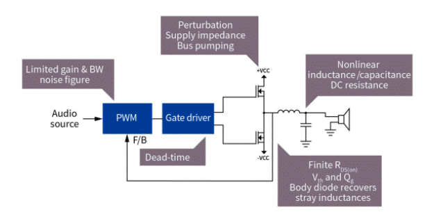
The Class D amplifier proposed in the 1950s has always used a pair of push/pull switching devices (Figure 1). The duty cycle of pulse width modulation (PWM) signals is controlled by the input audio signal, ensuring that the switching device is in an open or closed state, thereby keeping its linear region operation at the lowest level. This provides 100% theoretical efficiency and the possibility of zero distortion.
Figure 1: Basic block diagram of Class D amplifier design
Then, it turned out that the only available germanium transistors were not suitable for the requirements of this switching topology, and as a result, early amplifier designs were proven unsuccessful. However, the emergence of MOSFET technology has brought good luck to D-class designs. Nowadays, Class D amplifiers have found a home in various applications due to their electrical efficiency. In situations where compactness is a design requirement, such as in today‘s flat panel TVs and car audio consoles, it is also very popular because it usually does not require bulky heat sinks.
High electron mobility transistors (HEMTs) based on GaN provide a new technology for use as switches in D-class designs, with higher efficiency and improved audio quality.
Meets the requirements of Class D amplifiers
In theory, the high performance of Class D switching devices requires providing low on resistance to minimize I2R losses. The conduction resistance provided by GaN is much lower than that of Si MOSFET and can be achieved in a smaller bare chip area. Conversely, this is also reflected in small packaging, which designers can use to bring more compact amplifiers to the market.
Switching loss is another factor that needs to be fully considered. At medium to high power output levels, the performance of Class D amplifiers is exceptionally outstanding. However, due to losses in power devices, the lowest efficiency is achieved through the lowest power output.
To overcome this challenge, some Class D amplifier methods use two operating modes. This multi-level technology limits the output voltage that power devices can switch to when playing low volume audio. Once the output reaches a predefined threshold, the output voltage rail of the switch will increase, providing complete voltage swing. To further reduce the impact of switching losses, zero voltage switching (ZVS) technology can be used at low output levels and changed to hard switching at high power levels.
When implementing Si MOSFETs, the hard switching mode can cause charge accumulation in the body diode due to non-zero voltage at the output when the power device is turned off and on. The reverse recovery charge (Qrr) that needs to be established subsequently needs to be discharged, and its time needs to be incorporated into the PWM control implementation. In the design using GaN, this is not a problem as these transistors do not have an inherent body diode and therefore do not have Qrr. This result leads to overall higher efficiency, improved distortion, and clearer switching waveforms.
When the amplifier operates in ZVS mode, the switching loss and the resulting switching power loss can be effectively eliminated, as the output transition is achieved through the commutation of inductor current. However, like all half bridge designs, consideration needs to be given to the issue of direct connection, which is the moment when both high and low side switches are simultaneously connected. Usually, a short delay is inserted, known as the fade time, to ensure that one switching device is completely turned off before the other is turned on. It should be noted that this delay can affect the PWM signal, leading to audio output distortion. Therefore, the goal is to make it as short as possible to maintain audio fidelity. The duration of this delay depends on the output capacitance Coss of the power device. Although GaN transistors have not completely eliminated Coss, they are far lower than the Coss of Si MOSFET devices. As a result, a shorter blanking time results in less distortion of the amplifier when using GaN.
Despite some improvements, it is still necessary to process the energy stored in the capacitor and dissipate it in the next conduction cycle. However, due to the significant impact of these losses at higher switching frequencies, GaN based designs exhibit higher efficiency than Si based amplifiers.
Understand the benefits of implementing GaN
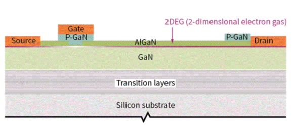
The terminal names of GaN HEMT transistors are the same as those of Si MOSFETs, with gate, drain, and source electrodes. Their extremely low resistance is achieved through a two-dimensional electron gas (2DEG) between the gate and source electrodes, effectively achieving short circuits due to the provided electron pool. When no gate bias is applied (VGS=0 V), the p-GaN gate stops conducting. Unlike its corresponding silicon, GaN HEMT is a bidirectional device. As a result, if the drain voltage is allowed to drop below the source voltage, the reverse current will flow. It should be noted that their clean switching is due to the lack of common body diodes in Si MOSFETs (Figure 2). This is the reason for many switching noises related to PN junctions.
Figure 2: Structure of GaN HEMT transistor
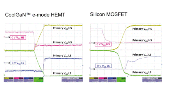
Figure 2a: Excellent switching characteristics of Class D amplifiers superior to Si MOSFETs
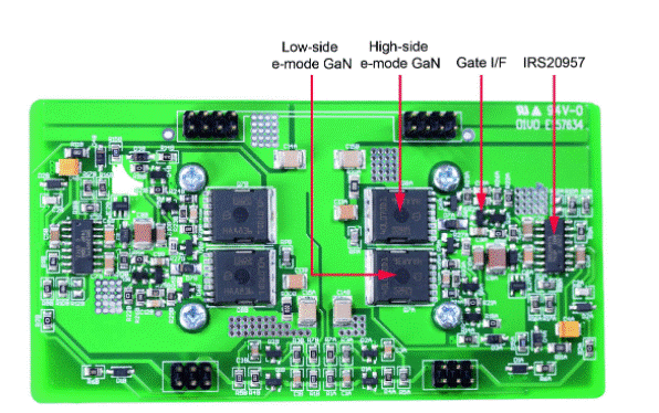
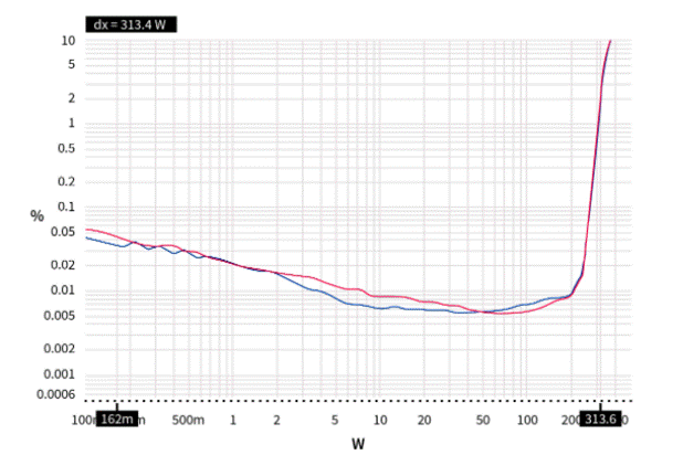
A Class D amplifier design has been implemented, which can convert 160 W power to 8 Ω without the need for a heat sink. One such prototype uses IGT40R070D1 E8220 GaN HEMT with a 200 V Class D driver IRS20957S (Figure 3). The RDS (on) (max) of this special switch is only 70m Ω. If used together with a heat sink, the amplifier can output up to 250 W of power and achieve a very impressive 0.008% THD+N at 100 W. Switching from ZVS to hard switch will cause a hump in the THD+N measurement value. Working at a frequency of 500 kHz, the design did not show significant distortion changes (occurring at a few watts), and the hard switching area remained quiet and very clean.
Figure 3: 250 W Class D amplifier design
Figure 3a: THD+N measurement
summarize
Over the years, due to continuous progress in optimizing performance, Si MOSFETs have provided excellent services for D-class amplifier designers. However, achieving further progress in their characteristics is challenging. In addition, further reduction of RDS (on) will lead to larger bare chip sizes, making it more difficult to build compact audio amplifier designs. However, GaN HEMT has overcome this limitation while also eliminating Qrr. In this way, combined with reduced Coss and the ability to operate at higher switching frequencies, it means that small, compact designs can be created without the need for heat sinks. The final THD+N measurement results also indicate the excellent audio performance that this new technology can achieve.
|
Disclaimer: This article is transferred from other platforms and does not represent the views and positions of this site. If there is any infringement or objection, please contact us to delete it. thank you! |


 Business consulting

 13823761625
 Mail me