


Bypass capacitor and coupling capacitor to stabilize voltage in the correct way
Time:2024-02-03
Views:232
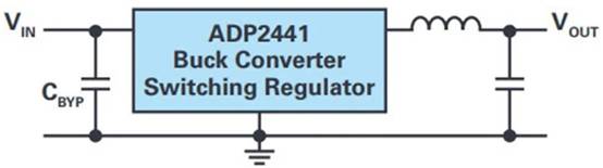
During the development of electronic products, bypass capacitors are often needed. Figure 1 shows a switching regulator that can generate low voltage from high voltage. In this type of circuit, bypass capacitance (CBYP) is particularly important. It must support the switching current on the input path to ensure that the power supply voltage is stable enough to support device operation.
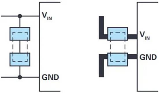
 •The position of the bypass capacitor on the circuit board is crucial for these components to achieve high efficiency. That is to say, it is very important to use the connection with the lowest possible parasitic inductance. The appropriate connection should be made on the same side of the circuit board where the circuit is located, as shown in Figure 2. In some special cases, it may be necessary to connect the bypass capacitor to the back of the circuit board. In this case, the connection with the lowest possible parasitic inductance shown in versions B, C, and D of Figure 3 should be chosen.
Figure 1. ADP2441 switch regulator with bypass capacitor CBYP at the input end.
Because the input capacitance in the step-down converter is a critical path (thermal loop) of this topology, the connection of CBYP must ensure as little parasitic inductance as possible. Therefore, the installation position of this component is crucial. The layout shown on the left side of Figure 2 is not very good. The wiring to the bypass capacitor is fine. The current flowing into the voltage converter does not directly flow into the bypass capacitor. The bypass capacitor only makes slight contact with the main circuit. This will increase the parasitic inductance generated by the capacitor and reduce the effectiveness of this component. It is recommended to use the layout shown on the right side of Figure 2, as the efficiency of the bypass capacitor is very high. The connection itself only generates a very small amount of parasitic inductance. From the figure, it can also be seen that the pin allocation of converters (such as switch regulators) will have an impact on the layout of the circuit board. From the right side of Figure 2, it can be seen that the distance between the VIN and GND pins is very close, which is closer than the layout on the left side that is not very good. In this way, the loop area between the bypass capacitor and the integrated circuit will be smaller.
Figure 2. Bypass capacitor connected in an unfavorable manner (left side) and bypass capacitor connected in an advantageous manner (right side).
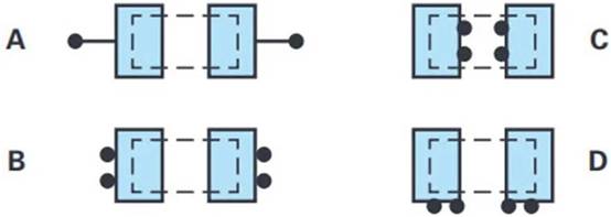
Because the connection of the bypass capacitor should ensure as little parasitic inductance as possible, it is recommended to place the bypass capacitor and switch regulator on the same side of the circuit board. However, in some applications, the front switch regulator can only be decoupled from the bypass capacitor at the bottom of the circuit board. This is true when there is not enough space to accommodate large decoupling capacitors. In this case, a through hole will be used to connect the capacitor. Unfortunately, through holes can generate parasitic inductance of several nanohertz. In order to minimize the impedance of this connection, various connection suggestions have been proposed, as shown in Figure 3.
Figure 3. When the bypass capacitor is connected to the through hole, there are multiple connection options.
• Version A is not very advantageous. In this option, a thin wire connection is used between the through hole and the bypass capacitor. This layout arrangement may also lead to an increase in parasitic inductance depending on the location of the path supported on the other side of the circuit board.
• Version A is not very advantageous. In this option, a thin wire connection is used between the through hole and the bypass capacitor. This layout arrangement may also lead to an increase in parasitic inductance depending on the location of the path supported on the other side of the circuit board.
• In version B, the through-hole position is closer to the bypass capacitor, so this connection is more advantageous. In addition, the two through holes are used in parallel. This can reduce the total inductance of the entire connection.
• Version C is more advantageous, as the connected circuit area is very small, resulting in only a very small amount of parasitic inductance. However, due to the small size of the bypass capacitor and the low cost of the manufacturing process, it is impossible or impossible to make through holes below the component.
• Version D provides a very interesting connection. According to the specific design of ceramic bypass capacitors, the parasitic inductance generated by horizontal connection to the circuit board may be minimized.
|
Disclaimer: This article is transferred from other platforms and does not represent the views and positions of this site. If there is any infringement or objection, please contact us to delete it. thank you! |


 Business consulting

 13823761625
 Mail me