


Design of ESD protection structures for touch sensing circuits
Time:2024-02-17
Views:211
The capacitive touch sensing detection button circuit is a type of circuit that is particularly sensitive to static electricity, so the selection of electrostatic discharge (ESD) protection structures is particularly important for this type of circuit. On the one hand, it is necessary to ensure that the selected ESD protection structure has sufficient anti-static ability, and on the other hand, this ESD protection structure cannot increase the area and cost of the chip too much. Based on this requirement, three ESD protection structures applied in capacitive touch sensing detection button circuits are introduced. This article mainly describes the circuit forms and layout of these three structures, with a focus on the improvements made to these three structures to meet the specific requirements of capacitive touch sensing detection button circuits. A comparison of the characteristics, chip area occupied, and anti-static ability test results of these three improved ESD protection structures is listed. The results indicate that the three improved ESD protection structures have achieved significant improvements in terms of protection capability, chip area utilization, and reliability.
Capacitive touch sensing detection button circuit is a relatively advanced integrated circuit product in the industry in recent years. This type of circuit usually has one or more highly sensitive sensing input terminals. In practical applications, the movement of charges is detected by the human finger approaching the chip, generating additional capacitance to change the frequency or duty cycle, thereby judging the human finger touch action and achieving button function. As is well known, the human body is the largest carrier of static electricity. Therefore, when the human fingers are close to the chip, a large amount of static electricity will be transmitted to the chip, which will generate potential destructive voltage, current, and electromagnetic field, thereby destroying the chip. This is the problem of electrostatic discharge (ESD). ESD is one of the most important reliability issues in metal oxide semiconductor (MOS) integrated circuits, especially for the capacitive touch sensing detection button circuit discussed in this article. In order to ensure high reliability, the ESD protection capability of such circuits usually requires reaching 8000 V, or even up to 10000 V. Therefore, effective ESD protection structures must be added to the circuit to meet the design requirements. In addition, this protective structure cannot occupy too much chip area, otherwise it will significantly increase chip costs and limit the promotion and application of chips. Therefore, how to choose a suitable ESD protection structure, which can protect this type of touch sensitive button detection circuit without increasing the chip cost too much, is a crucial issue in the design of such circuits.
This article introduces three ESD protection structures applied in the capacitive touch sensing detection button circuit developed by the author. These three protection structures are comprehensively improved based on the traditional ESD structure and combined with the specific characteristics of capacitive touch sensing detection button circuits, in order to achieve the requirement of protecting the circuit and increasing the chip area as little as possible. These structures are also applicable to other similar circuits, hoping to provide some reference designs for engineers engaged in integrated circuit design when considering ESD issues.
1. 3 ESD protection structures
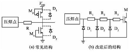
1.1. ESD protection structure with diode and resistor
Figure 1 (a) is the most common ESD protection structure in MOS integrated circuits. This structure needs to be inserted at every solder joint of the circuit to protect the two MOS transistors, Mp and Mn, in the diagram. This structure includes a PMOS transistor Mp directly connected to the solder joint and a NMOS transistor Mn short connected to the gate and source. The Mp and Mn transistors can be equivalent to two diodes D1 and D2. In practical applications, a large amount of static electricity will be introduced at the solder joint. According to the principle of crystal tubes, this large static electricity will cause avalanche breakdown of the Mp and Mn transistors. By inserting the ESD protection structure in Figure 1 (a), before the large static electricity reaches Mp and Mn, it first causes two diodes D1 and D2 to reverse breakdown, forming a current path to the power supply and ground, releasing the large current; In addition, resistor R plays a current limiting role. These two measures have played a role in protecting Mp and Mn. The ESD protection capability of this ESD protection structure is usually between 2000-3000V. In order to further improve the ESD protection capability, this structure has been improved in the capacitive touch sensing detection button circuit, as shown in Figure 1 (b). Figure 1 (b) shows an ESD protection structure with a three-level diode resistor network for NMOS transistors, similar to the protection structure for PMOS transistors. The principle of each stage is similar to Figure 1 (a), but this structure can provide multiple discharge paths by utilizing the current limiting and voltage dividing effects of the three-level resistor and diode network, thereby gradually releasing and amplifying the current, and improving the ESD protection ability. Taking the MOSFET Mn in Figure 1 (b) as an example, illustrate how to select the circuit structure parameters for this improved ESD protection structure. The gate breakdown voltage of Mn is 12.5V. According to the ESD protection principle, the voltage that falls on the gate of Mn after passing through multiple stages of current limiting resistors must be less than the gate breakdown voltage of this transistor in order to protect the circuit. Through calculation, the use of a three-level diode and resistance network structure can achieve the purpose of protecting Mn, where each stage of current limiting resistor has a value of 100 Ω. The D1, D2, and D3 diodes can also use Figure 1 (a) The MOSFET with gate and source short circuited as shown in.
Figure 1: ESD protection structure with diode and resistor
1.2 ESD protection structure of thyristor rectifier
Figure 2 (a) is a longitudinal sectional view of the ESD protection structure of a silicon controlled rectifier (SCR), and Figure 2 (b) is an equivalent circuit diagram of this structure.
In Figure 2 (b), Mp is a PMOS transistor with a gate and source short circuited, providing ESD protection; Q1 is a pnp type transistor, with an emission region consisting of a p+diffusion region within an n-well, where the n-well is its base region and the p-substrate serves as the collector region; The other Q2 is an npn type transistor, with n+outside the well as its emitting region, p substrate as its base region, and n well as the collector region. The above two tubes form a 4-layer semiconductor device called a thyristor rectifier. These four layers are sequentially the p+diffusion zone, n well, p substrate, and n+diffusion zone. This pnpn structure has a positive feedback between npn and pnp, providing a good ESD release pathway and demonstrating significant ESD protection performance. Therefore, inserting such a structure at every solder joint of the chip can provide the highest ESD protection capability with the smallest layout area. In Figure 2 (b), R1 is the n-well contact resistance, and R2 is the p-substrate contact resistance.
According to the principles of semiconductor devices, the 4-layer structure mentioned above serves as an ESD protection device, and its initial conduction voltage is equivalent to the breakdown voltage between the n-well and p-substrate under MOS technology. Due to the low doping concentration of the n-well, which is determined by the semiconductor process, the breakdown voltage between it and the p-substrate can reach 30-50V. Such a high breakdown voltage requires an additional secondary protection structure in the ESD protection design of the SCR structure, as indicated in Figure 2 (b). This is because the gate breakdown voltage of the MOS transistor M that needs to be protected in Figure 2 (b) is only about 12.5V, while the SCR needs to conduct above 30V. Before the ESD voltage rises to 30V, this SCR structure is closed. At this time, the M transistor that the SCR device needs to protect has long been damaged by the ESD voltage, so a secondary protection structure must be added. By utilizing this secondary protection structure, the SCR structure can be triggered to conduct before it is destroyed by ESD, thereby releasing ESD current. As long as the SCR structure conducts, its low holding voltage will clamp the ESD voltage at a very low value. Therefore, this SCR structure can effectively protect the M transistor. But this additional secondary protection structure will inevitably result in an increase in chip area, leading to an increase in chip costs.
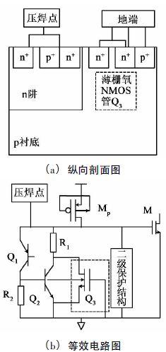
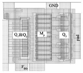
Figure 2: Longitudinal sectional view and equivalent circuit diagram of SCR ESD protection structure
To address this issue, an improved SCR ESD protection structure has been adopted in the capacitive touch sensing detection button circuit. Add a thin gate oxygen NMOS transistor Q3 as shown in the dashed box in Figure 2 (b) to this structure. According to the transistor principle, the breakdown voltage is directly related to the gate oxygen. This NMOS transistor spans across the interface between the n-well and p-substrate, reducing the initial conduction voltage of the SCR structure to 10-15V. This allows the SCR structure to effectively protect the M transistor inside the circuit without the need for additional secondary protection structures, thereby reducing the chip area. The conduction process of the SCR structure is described as follows: when the embedded thin gate NMOS transistor Q3 undergoes reflux breakdown, it triggers the current to flow from its gate to the p-substrate, which causes the current to flow from the n-well to the p-substrate, thereby triggering the conduction of the SCR structure. In order to prevent the SCR structure from conducting under normal operating conditions of ordinary MOSFETs, the gate of the embedded thin gate NMOS transistor Q3 must be connected to ground to keep the NMOS transistor turned off, as shown in Figure 2 (b).
Figure 3 shows the layout of the improved SCR ESD protection structure, including Q1 and Q2 as ESD protection devices, PMOS transistor Mp with a aspect ratio of 180/1, and thin gate transistor Q3 as ESD secondary protection device. In the figure, VDD is the power terminal connected to the transistor, and GND is the ground terminal connected to the transistor.
Figure 3 Improved SCR ESD Protection Structure Layout
1.3. Full chip ESD protection structure
Figure 4 shows a full chip ESD protection circuit structure. This protection structure consists of two parts: ESD discharge and protection structure and conventional diode protection structure. The ESD discharge and protection structure consists of an RC network, two logic control tubes Mp and Mn, and an ESD current discharge tube TESD. The principle of this part is summarized as follows: The damage of ESD to the circuit is mainly caused by the irreversible breakdown of the circuit‘s pn, which leads to circuit leakage. When ESD voltage appears on the VDD network, the initial voltage at point Vx in the figure is zero. Due to the inertia of the capacitor, the voltage at both ends cannot suddenly change. Therefore, the Mp transistor conducts, and the Vg terminal voltage will increase with the ESD voltage. The TESD transistor conducts, providing a discharge path to the ground for the ESD current. The thin gate oxygen of TES D determines that the voltage at point Vg in the figure cannot rise too high, otherwise it will breakdown the gate oxygen and damage the device. Therefore, when charging the RC network, the voltage at the Vx end is raised to limit the increase in Vg. The RC charging time must be able to ensure that the ESD can be fully discharged before turning off the Mn transistor, which generally requires around 200ns. The design of the TESD transistor is required to be able to carry large currents, so sufficient gate width to length ratio must be designed. Under normal circumstances, the gate voltage of the TESD transistor is 0V, which is actually turned off, so it does not affect the normal operation of the chip.
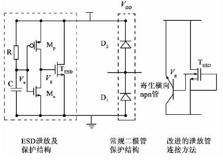
Figure 4 Full chip ESD protection circuit structure
This full chip ESD protection structure can effectively improve the ESD protection capability of the circuit, but when the semiconductor process reaches the deep submicron stage, in order to prevent hot carrier effects, shallow doped drain (LDD) structures are used at the source and drain ends of MOS. The TESD tube in Figure 4 adopts an LDD structure. When the TESD tube conducts and releases ESD current, a large current passes through the surface of the tube, making it easy to damage shallow impurities with shallow junction depth, thereby limiting the protective ability of this full chip ESD protection structure.
An improved full chip ESD protection structure was adopted in the capacitive touch sensing detection button circuit, which improved the connection method of the ESD current discharge tube TESD, as shown in Figure 4. After improvement, the gate of the TES D transistor is grounded, while the Vg output is connected to the substrate of the TES D transistor, while the other device structures and parameters remain unchanged. Compared with the usual full chip ESD protection structure, this improved full chip ESD protection structure introduces parasitic lateral NPN transistors, as shown in Figure 4.
In this improved full chip ESD structure, when ESD voltage appears on the VDD network, it will cause a change in Vg voltage. Due to the presence of voltage, it will cause the migration of electrons on the substrate and form a current. After the current flows through the substrate resistance, it will raise the base voltage of the parasitic NPN transistor, ultimately triggering the conduction of this NPN transistor. At this time, the ESD current flows through the NPN transistor on the substrate rather than on the surface of the MOS transistor, The TESD tube is not turned on, but instead uses its parasitic lateral NPN tube to discharge ESD current, while the LDD structure is not damaged by ESD current, which can greatly improve the ESD protection capability of this protective circuit.
The dashed box in Figure 5 shows the layout of this improved full chip ESD protection structure. The figure shows the positions of the logic control transistor Mp, Mn, and RC networks, as well as the most important thin gate transistor TESD, where the capacitor and its underlying well resistance form the ESD detector. From Figure 5, it can be seen that the area occupied by a full chip ESD protection structure is only slightly larger than the area of a solder joint. This means that inserting this full chip ESD protection structure into a certain chip will not cause a significant increase in the chip‘s area, but it can greatly improve the chip‘s ESD protection ability.
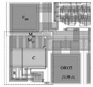
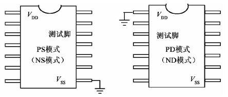
Figure 5 Layout of Full Chip ESD Protection Structure
2. Comparison and Test Results of Three ESD Protection Structures
2.1 Comparison of the advantages and disadvantages of three structures under different ESD testing modes
For each port of the chip, there are four ESD testing modes, which are tested for ± VDD and ± VSS modes, respectively called PS mode for all test pin pairs+VDD, NS mode for all test pin pairs - VDD, PD mode for all test pin pairs+VSS, and ND mode for all test pin pairs - VSS. As shown in Figure 6, for one of the test pins, a positive or negative ESD voltage is applied, and all other untested ports are suspended. Only when all four modes successfully pass a certain voltage test (such as 4000V) can the ESD protection capability of this port be considered to have reached 4000V
Figure 6: Four ESD testing modes
For ESD protection structures with diodes and resistors, the diodes are typically implemented using gate grounded NMOS transistors and gate grounded PMOS transistors. The circuit using this ESD protection structure generally has a higher ESD protection ability for the NS and PD testing modes, while the ESD protection ability for the ND and PS testing modes is much worse. This is because in NS test mode, when a negative ESD voltage is applied to a test pin, the diode parasitized by the NMOS transistor conducts forward. Similarly, in PD mode, the VDD terminal is grounded, and when a positive ESD voltage is applied to a test pin, the diode parasitized by the PMOS conducts forward, as shown in Figure 1 (b). In ND and PS modes, parasitic diodes require reverse breakdown to discharge ESD current. The ESD energy that a specific device can withstand is fixed, and the forward conduction voltage of the diode is about 0.7V, which is much lower than its reverse breakdown voltage. Therefore, the ESD discharge current that the diode can withstand when conducting forward is also much greater than when conducting reverse, that is, the ESD voltage is much higher than when conducting reverse. Therefore, the poor ESD protection capability in ND and PS modes is a disadvantage of this protection structure.
Similarly, the ESD protection structure of thyristor rectifiers also has the same problem. The full chip ESD protection circuit can precisely solve this problem, demonstrating the superiority of this structure over the first two structures. The principle is as follows: Taking PS mode as an example, the power pin is suspended and the ground pin is connected to a low level. Without a full chip ESD protection circuit, the D1 parasitic diode will reverse breakdown and discharge the ESD current. Now, the ESD voltage will be charged to the VDD network through D2, as shown in Figure 4, and then discharged to ground through the ESD protection circuit. The above ESD leakage methods avoid the occurrence of D1 reverse breakdown, and similarly, ND mode can also be analyzed using this approach.
2.2 Comparison of chip area occupied by three different structures and ESD withstand voltage test results
Applying the above three structures to the design of capacitive touch sensing button detection circuit, the chip uses 0.35 μ The MOS process has a total of 10 solder joints. The chip area occupied by the three structures is shown in Table 1. In the table, A represents the chip area occupied by the ESD structure, and VESD represents the voltage used in the ESD withstand voltage test.
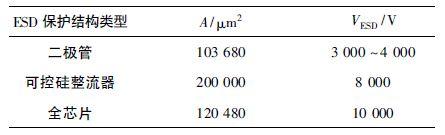
Table 1: Chip area occupied by three ESD protection structures and actual ESD withstand voltage test results
The ESD withstand voltage test was conducted on chips using three improved ESD protection structures, and the results are shown in Table 1. From the comparison results in Table 1, it can be seen that the chip area occupied by the full chip ESD protection structure is 16800 more than that of the diode ESD protection structure μ M2, the proportion of area increase is 16%, but the ESD protection ability has increased by more than twice; Compared with the thyristor rectifier ESD protection structure, the full chip ESD protection structure only occupies 60% of the chip area of the thyristor rectifier ESD protection structure, but the ESD protection ability is increased by 2000V, indicating that the full chip ESD protection structure has the best ESD protection ability.
2.3 Test results of ESD protection capability for three structures
Using the industrial testing standard HBMMIL-STD-883F3.15.7, one of the ESD models, to test the ESD protection capability of the capacitive touch sensing detection button circuit using the three improved ESD protection structures mentioned above. Taking PS mode as an example, the specific testing method is as follows: prepare 3 samples for each circuit, and these 3 samples must first pass the functional test; The power pin is suspended, the ground pin is connected to a low level, and all other pins are also suspended. A positive voltage is applied to one of the test pins to equivalent the positive ESD voltage that the actual circuit is subjected to. The starting voltage is 500V, and for each subsequent test, the voltage increases by 500V, which means the step voltage is 500V; Then monitor the current voltage curve of the test pin before and after applying ESD voltage, usually using the envelope method to determine the changes in the current voltage curve of the test pin before and after applying ESD voltage. When the relative envelope line is less than 15%, it is judged that there is no change in the current voltage curve before and after applying ESD voltage, and the pin can also withstand higher ESD voltage. Continue to increase the voltage upwards until it exceeds the range of 15%. For example, if it is added to 4500V and the relative envelope line exceeds 15%, it indicates that the test pin has exceeded the ESD withstand range. At this point, the previous level of the applied ESD voltage of 4500V, which is 4000V, is the highest ESD voltage that the test pin can withstand; Perform tests on the test pin in three other modes, including NS, PD, and ND. If all four modes can pass 4000V and the circuit function remains unchanged after ESD striking, all three samples need to repeat this test to indicate that the ESD withstand voltage of this pin is 4000V
The ESD level is usually divided into three levels: the first level is 0-199V; The secondary voltage ranges from 2000 to 3999V; The third level is 4000-8000V. For some special applications, the ESD withstand voltage requirement exceeds 10000V. That is to continue to increase the ESD voltage on the basis of the third level until the applied voltage exceeds 10000V, and the current voltage curve of the test pin does not change, indicating that the ESD withstand voltage of the chip can reach up to 10000V
3. Conclusion
The capacitive touch sensing detection button circuit requires a particularly high ESD protection capability, therefore an effective ESD protection structure must be adopted. This article lists three ESD protection structures, including diodes with resistors, controllable silicon rectifiers, and full chips, and focuses on the structure and process characteristics of capacitive touch sensing detection button circuits. Improvement measures for these three protection structures are proposed. The results show that the three improved ESD protection structures have greatly improved in terms of protection ability, chip area utilization, and reliability. Among them, the full chip ESD protection structure occupies the smallest chip area and has the best ESD protection ability for all ESD testing modes. This structure can be extended to the design of ESD protection structures for other types of integrated circuits.
|
Disclaimer: This article is transferred from other platforms and does not represent the views and positions of this site. If there is any infringement or objection, please contact us to delete it. thank you! |


 Business consulting

 13823761625
 Mail me