


Prevent LED driver output from short circuiting to ground
Time:2024-03-02
Views:177
In applications such as automotive LED lighting, due to the driver‘s usual distance from the LED, it is necessary to add short-circuit protection function. JOHN RICE introduces in this article how to prevent the output of LED drivers from short circuiting to ground.
Asynchronous, boost, and power conversion topologies are often used in applications such as LED drives. In these applications, the input voltage (VIN) is not sufficient to forward bias a series/parallel LED string. This inductor switch topology generates the necessary compliance voltage for LED current regulation and is commonly used in LCD backlight applications. For example, in LED matrix applications such as interior and exterior lighting in cars far from the driver, there is a risk of output short circuit to ground, which can lead to catastrophic consequences. Limiting current and operating protective circuits as electronic circuit breakers can prevent these catastrophic faults.
As shown in Figure 1, the input of the boost converter is physically connected to its output through a boost inductor (L1) and a boost diode (D1). Therefore, a short circuit on the output can saturate the boost inductor, causing a current spike that is enough to damage the boost diode. Even worse, this short circuit situation can also interfere with all devices connected to the input, including pulse width modulation (PWM) controllers. It is obvious that when using this topology, some type of circuit protection is required to power remote LEDs. Next, we will consider designing a multi-purpose, low-cost circuit that can be optimized to protect the boost converter and prevent short-circuit load conditions at the input end. In addition, we will verify the required response through an analog circuit.
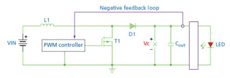
Figure 1. LED driver circuit based on non isolated boost topology
Current limiters and electronic circuit breakers
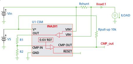
Shunt Monitor (CSM) is a high-precision, high gain differential current sensing amplifier commonly used to monitor input and output currents. Figure 2 shows its typical configuration. This specific device integrates an open drain comparator; This comparator can be set to jump, latch, and reset on a pre-set line current.
Figure 2 A diversion monitor component has added protection function
The output of this comparator can be used to control an external MOSFET switch that can interrupt the load short circuit within a few milliseconds. In addition to interrupting input current in case of output failure, analog output can also solve the so-called "negative input impedance" problem of switch regulators, preventing input current from increasing with decreasing input voltage.
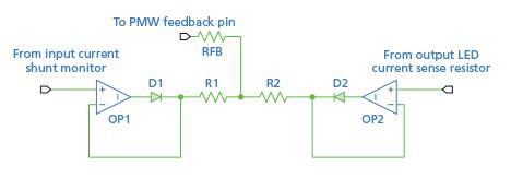
By connecting the input current and output current in a logical OR configuration, input clamping can be achieved. As shown in Figure 3, its purpose is to generate a composite feedback signal that drives the PWM controller. Then, CSM renders the output current feedback invalid and forces the LED current to decrease when the input voltage drops below a preset level, thereby limiting the input current.
Figure 3 Input current limiter relies on sensing input and output currents
Circuit operation
Figure 4 shows the circuit implementation of a boost converter LED driver with output short-circuit protection function. The Osram Opto Semiconductors LED displayed in the circuit is a device designed for automotive headlight applications, which is actually a single piece, LED located on an insulated metal substrate. This device has a rated surge current of 2A (less than 10 μ s) And a typical forward voltage of 18V at a current of 1A. The DC/DC boost converter senses the forward LED current on the feedback pin and fully adjusts the output voltage to adjust the LED current. The LED current is set by a sensing resistor (RSNS), whose value is proportional to the internal bandgap reference of the PWM converter (RSNS=VREF/ILED). Using a boost converter with a low reference voltage can easily achieve higher converter efficiency and reduce component thermal stress.
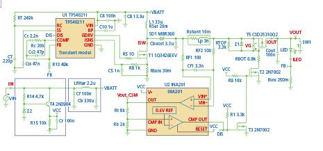
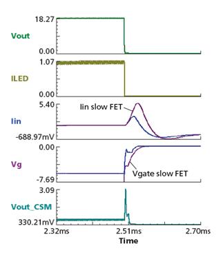
Figure 4. LED Booster Driver Circuit with Short Circuit Load Fault Protection Function
Although the lifespan can reach over 50000 hours, LEDs are highly sensitive to temperature and electrical overstress, and their dynamic impedance characteristics often pose challenges for the selection of switch regulator components and the design of control loops. This operating manual explains these selection and design challenges. According to this method, the circuit simulation shown in Figure 4 was developed to analyze the complexity of the LED driver/protection circuit and predict the circuit operation under various working conditions.
The PWM controller selected for this analysis has a feedback reference voltage of 0.26V. So, when the LED current is 1A, the power dissipation of the LED sensing resistor is only 0.26W. Due to the CSM having a gain of 50, a much smaller sensing resistor is needed to sense the output current. When the current flowing through the CSM shunt resistor exceeds the limit set by the CSM sensing resistor, the CSM gain and comparator threshold (R, R) interrupt the load current of the PMOS conducting transistor, thereby playing the role of an electronic circuit breaker.
You can reset the latch output by switching the RESET pin to a low level. However, considering the purpose of this article, RESET has been disabled to test response speed. The response speed and peak current depend on many variables. These variables include component selection, CSM bandwidth, noise filter, output capacitor, FET selection, and output boost inductor. These factors combined will affect the output impedance of the converter. To accurately evaluate the operating mode, we conducted simulations with a maximum time step of 50ns and a DC relative tolerance set at 0.001%. This analysis runs on TINA-TI, a free Berkeley SPICE 3f5 compatible simulator. The 5ms simulation of a boost converter with a working frequency of 300kHz can start to a stable state in just 30 seconds.
Where to place CSM
CSM can be placed on the input or output of the boost converter. In this simulation, the CSM is placed on the output and senses current through a 10m Ω shunt resistor parallel to the output PMOS conducting element (T5). According to the placement of the CSM, this circuit can prevent internal and/or external short circuits. However, CSM must be designed to have sufficient common mode range (CMR) under all operating conditions.
If placed on the input of the boost converter, a CSM with a lower CMR can be selected. However, placing the CSM on the output can avoid the boost inductor and help accelerate the response time to short circuit situations. No matter where the CSM is placed, an RC filter should be used to attenuate noise and ringing that may occur due to sudden di/dt events in the shunt resistor. A small 100 resistor and differential capacitor can be placed with a time constant three times larger than the estimated shunt Lp/R time constant, where Lp is the parasitic parallel inductance. Due to the negative impact of noise filters on the gain error and bandwidth of CSM, it is important to maintain a low value of the filter.
Simulation results
Figure 5 shows the simulation results. Vg is the control voltage to PMOS FET and is set to -6V under normal conditions. Optimization needs to be based on the threshold voltage, gate charge, and saturation characteristics of FETs. Minimizing the voltage on the gate to the maximum extent can improve the response time, and pull-up resistors should be selected to minimize the interruption cycle as much as possible. It should be noted that the input current and gate voltage are displayed in high gate charge (purple) and low gate charge (blue) MOSFETs.
Figure 5. Standard wired and wireless networks will carry and transmit relatively simple commands and data between physical building systems and building management equipment
It is evident that lower gate charge devices minimize the visible current on the input to the greatest extent possible. Choosing MOSFETs and gate drive circuits to achieve optimal response is a crucial design consideration, as this design limits di/dt and meets the requirements for safe operation of MOSFETs. These complex design considerations are not so easy to analyze; Therefore, it is best to simulate and confirm them on the workbench.
Provide specialized testing software on certain oscilloscopes such as Tektronix products to calculate the switching power loss relative to the MOSFET safe operating curve. This simulation suggests a response duration of less than 2 μ s. This can obtain an input current of less than 6A before the current is interrupted. The selection of interrupt FET will affect the peak input and output currents. A high-performance, hot swappable controller that drives high-end NMOS devices is another option and can achieve interruption times of less than 250ns. These devices have been optimized for backplane hot swappable card insertion, but can provide a solution with higher performance than the one shown here.
Avoided faults
This circuit demonstrates and simulates interruption scenarios, as well as limits the input/output current of the boost converter LED driver under variable load conditions. This circuit has been optimized to be suitable for automotive LED headlight driver applications. We have demonstrated that achieving optimal circuit response time requires careful analysis and component selection. Integrating these sensitivities into a comprehensive time-domain circuit simulation helps to understand the operational status of the circuit under different operating conditions and component selection.
The specialized hot swappable controllers provided have specialized features and optimized performance, which should be taken into consideration in design. In any case, careful analysis is necessary when executing a circuit to interrupt or limit power supply. Designing a robust and durable protection circuit for LED drivers is a complex task, and software tools such as TINA-TI, SPICE, and WEBENCH can provide assistance in accelerating analysis and design.
|
Disclaimer: This article is transferred from other platforms and does not represent the views and positions of this site. If there is any infringement or objection, please contact us to delete it. thank you! |


 Business consulting

 13823761625
 Mail me