


Detailed explanation of MOS transistor working principle diagram - MOS transistor working principle circuit diagram and structural analysis - MOS transistor
Time:2024-03-23
Views:107
Detailed explanation of MOS transistor working principle diagram
MOSFET is a type of FET (another type is JFET) that can be manufactured as either enhanced or depleted, with a total of four types: P-channel or N-channel. However, only enhanced N-channel MOSFETs and enhanced P-channel MOSFETs are actually used, so NMOS or PMOS is usually referred to as these two types.
For these two types of enhanced MOSFETs, NMOS is commonly used. The reason is that the conduction resistance is small and easy to manufacture. So in the applications of switch mode power supplies and motor drives, NMOS is generally used. In the following introduction, NMOS is also mainly used.
There is parasitic capacitance between the three pins of the MOS transistor, which is not what we need, but is caused by manufacturing process limitations. The existence of parasitic capacitance makes it more troublesome to design or select driving circuits, but it cannot be avoided. We will explain it in detail later.
On the working principle diagram of the MOS transistor, it can be seen that there is a parasitic diode between the drain and source. This is called a body diode, which is very important in driving inductive loads (such as motors). By the way, body diodes only exist in a single MOSFET and are typically not present within integrated circuit chips.
Detailed explanation of MOS transistor working principle diagram and power switch circuit

It generally has two types: depletion type and enhancement type. This article uses enhanced MOS
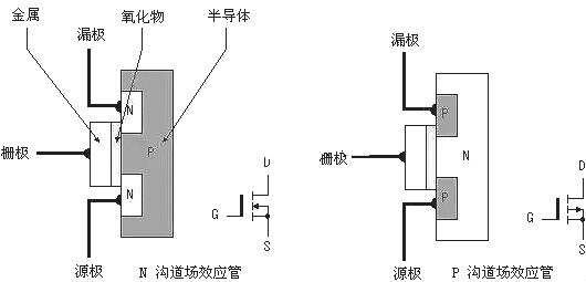
The internal structure of MOS transistor is shown in the working principle diagram of MOS transistor. It can be divided into NPN type and PNP type. The NPN type is commonly referred to as the N-channel type, while the PNP type is also known as the P-channel type. As shown in the figure, for N-channel field-effect transistors, the source and drain are connected to the N-type semiconductor, while for P-channel field-effect transistors, the source and drain are connected to the P-type semiconductor. We know that a typical transistor controls the output current by the input current. But for field-effect transistors, their output current is controlled by the input voltage (or electric field), which can be considered as having very little or no input current. This makes the device have a high input impedance, which is also why we call it a field-effect transistor.
The internal structure of MOS transistor is shown in the working principle diagram of MOS transistor. It can be divided into NPN type and PNP type. The NPN type is commonly referred to as the N-channel type, while the PNP type is also known as the P-channel type. As shown in the figure, for N-channel field-effect transistors, the source and drain are connected to the N-type semiconductor, while for P-channel field-effect transistors, the source and drain are connected to the P-type semiconductor. We know that a typical transistor controls the output current by the input current. But for field-effect transistors, their output current is controlled by the input voltage (or electric field), which can be considered as having very little or no input current. This makes the device have a high input impedance, which is also why we call it a field-effect transistor.
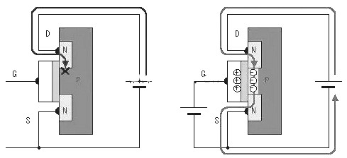
To explain the working principle of MOS transistors, let‘s first understand the working process of a diode containing only one P-N junction. As shown in the figure, we know that when a forward voltage is applied to the diode (P terminal is connected to the positive pole, N terminal is connected to the negative pole), the diode conducts and there is current flowing through its PN junction. This is because when the P-type semiconductor terminal has a positive voltage, the negative electrons inside the N-type semiconductor are attracted and surge towards the P-type semiconductor terminal with a positive voltage applied, while the positive electrons inside the P-type semiconductor terminal move towards the N-type semiconductor terminal, forming a conducting current. Similarly, when a diode is subjected to a reverse voltage (with the P-terminal connected to the negative terminal and the N-terminal connected to the positive terminal), the voltage is negative at the P-type semiconductor terminal. Positive electrons are gathered at the P-type semiconductor terminal, while negative electrons are gathered at the N-type semiconductor terminal. The electrons do not move, and there is no current passing through the PN junction, causing the diode to cut off.

For MOS transistors (see figure), when there is no voltage at the gate, as analyzed earlier, there will be no current flowing between the source and drain. At this point, the MOS transistor is in the cutoff state (Figure a). When a positive voltage is applied to the N-channel MOSFET.
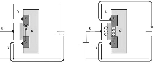
When on the gate of the MOS transistor, due to the effect of the electric field, the negative electrons of the source and drain of the N-type semiconductor are attracted and surge towards the gate. However, due to the obstruction of the oxide film, electrons gather in the P-type semiconductor between the two N-channels (see Figure b), forming a current that conducts between the source and drain. We can also imagine that there is a channel between two N-type semiconductors, and the establishment of gate voltage is equivalent to building a bridge between them. The size of the bridge is determined by the gate voltage. The figure shows the MOS transistor of the P-channel.
When on the gate of the MOS transistor, due to the effect of the electric field, the negative electrons of the source and drain of the N-type semiconductor are attracted and surge towards the gate. However, due to the obstruction of the oxide film, electrons gather in the P-type semiconductor between the two N-channels (see Figure b), forming a current that conducts between the source and drain. We can also imagine that there is a channel between two N-type semiconductors, and the establishment of gate voltage is equivalent to building a bridge between them. The size of the bridge is determined by the gate voltage. The figure shows the MOS transistor of the P-channel.
The working process of MOS transistor working principle diagram is similar to here and will not be repeated.
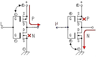
Below is a brief description of the working process of an application circuit composed of C-MOS field-effect transistors (enhanced MOSFETs) (see figure). The circuit combines an enhanced P-channel MOSFET with an enhanced N-channel MOSFET. When the input terminal is at low voltage, the P-channel MOSFET conducts and the output terminal is connected to the positive pole of the power supply. When the input terminal is at high voltage, the N-channel MOSFET conducts, and the output terminal is connected to the power ground. In this circuit, P-channel MOSFETs and N-channel MOSFETs always operate in opposite states, with opposite phase inputs and outputs. Through this working method, we can obtain a larger current output. At the same time, due to the influence of leakage current, the gate voltage is not yet 0V. Usually, when the gate voltage is less than 1 to 2V, the MOSFET is turned off. The turn off voltage of different field-effect transistors varies slightly. It is precisely because of this that the circuit will not cause a power short circuit due to the simultaneous conduction of two tubes.
From the above analysis, we can draw the working process of the MOS transistor circuit in the MOS transistor working principle diagram (see figure). The working principle is the same as before.
MOSFET application circuit
The most significant feature of MOSFETs is their excellent switching characteristics, which is why they are widely used in circuits that require electronic switches. Common applications include switch mode power supplies, motor drives, and lighting dimming.
There are several special requirements for MOS drivers nowadays:
1. Low voltage applications
When using a 5V power supply, if a traditional MOSFET working principle diagram totem pole structure is used, the actual final voltage applied to the gate is only 4.3V due to a voltage drop of about 0.7V in the transistor. At this point, choosing MOSFETs with a nominal gate voltage of 4.5V poses certain risks.
The same problem also occurs in situations where 3V or other low-voltage power sources are used.
The same problem also occurs in situations where 3V or other low-voltage power sources are used.
2. Wide voltage application
The input voltage is not a fixed value, it can vary over time or other factors. This change causes the driving voltage provided by the PWM circuit to the MOSFET to be unstable.
In order to ensure the safety of MOSFETs under high gate voltage, many MOSFETs have built-in voltage regulators that forcibly limit the amplitude of the gate voltage. In this case, when the provided driving voltage exceeds the voltage of the voltage regulator, it will cause significant static power consumption.
At the same time, if the principle of resistance voltage division is simply used to reduce the gate voltage, the MOSFET will work well when the input voltage is relatively high, but when the input voltage decreases, the gate voltage will be insufficient, causing incomplete conduction and increasing power consumption.
3. Dual voltage application
In some control circuits, the logic part uses typical 5V or 3.3V digital voltage, while the power part uses 12V or even higher voltage. Two voltages are connected in a common ground manner.
This requires the use of a circuit that allows the low-voltage side to effectively control the high-voltage side MOSFETs, while the high-voltage side MOSFETs will also face the issues mentioned in 1 and 2.
In these three cases, the totem pole structure cannot meet the output requirements, and many existing MOS driver ICs do not seem to include gate voltage limiting structures.
So I designed a relatively universal circuit to meet these three requirements.
Summary 1: Summary of the causes of MOS tube heating
This requires the use of a circuit that allows the low-voltage side to effectively control the high-voltage side MOSFETs, while the high-voltage side MOSFETs will also face the issues mentioned in 1 and 2.
In these three cases, the totem pole structure cannot meet the output requirements, and many existing MOS driver ICs do not seem to include gate voltage limiting structures.
So I designed a relatively universal circuit to meet these three requirements.
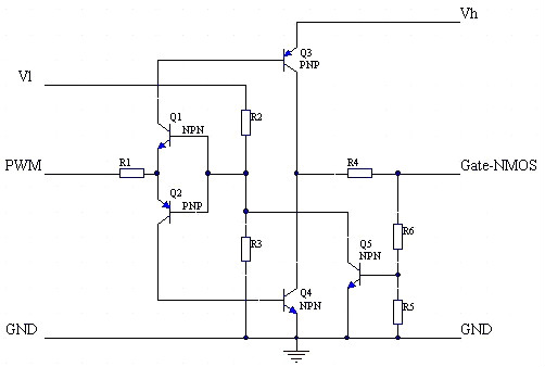
The working principle diagram of MOSFET is as follows:
Driver circuit for NMOS
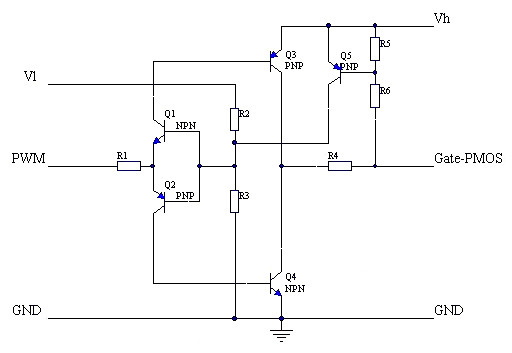
Driver circuit for PMOS
A Simple Analysis of NMOS Driver Circuit
A Simple Analysis of NMOS Driver Circuit
Vl and Vh are low-end and high-end power supplies, respectively. The two voltages can be the same, but Vl should not exceed Vh.
Q1 and Q2 form an inverted totem pole to achieve isolation while ensuring that the two drive tubes Q3 and Q4 do not conduct simultaneously.
erate at a position where the PWM signal waveform is relatively steep.
Q3 and Q4 are used to provide driving current. When conducting, Q3 and Q4 have a minimum voltage drop of only one Vce relative to Vh and GND, which is usually only about 0.3V, much lower than the Vce of 0.7V.
R5 and R6 are feedback resistors used to sample the gate voltage. The sampled voltage generates a strong negative feedback on the base of Q1 and Q2 through Q5, thereby limiting the gate voltage to a finite value. This value can be adjusted through R5 and R6
inally, R1 provides a base current limitation for Q3 and Q4, while R4 provides a gate current limitation for MOSFETs, that is, an Ice limitation for Q3 and Q4. If necessary, parallel acceleration capacitors can be connected to R
This circuit provides the following features:
1. Use low-end voltage and PWM to drive high-end MOSFETs.
2. Use a small amplitude PWM signal to drive MOSFETs with high gate voltage requirements.
3. Peak limit of gate voltage
4. Input and output current limitations
5. By using appropriate resistors, very low power consumption can be achieved.
6. PWM signal inverted. NMOS does not require this feature and can be solved by pre installing an inverter.
When designing portable devices and wireless products, improving product performance and extending battery life are two issues that designers need to face. DC-DC converters have the advantages of high efficiency, large output current, and low static current, making them very suitable for supplying power to portable devices.
The main development trends of DC-DC converter design technology:
(1 ) High frequency technology: With the increase of switching frequency, the volume of the switching converter also decreases, the power density is greatly improved, and the dynamic response is improved. The switching frequency of low-power DC-DC converters will increase to the megahertz level.
(2) Low output voltage technology: With the continuous development of semiconductor manufacturing technology, the working voltage of microprocessors and portable electronic devices is getting lower and lower, which requires future DC-DC converters to provide low output voltage to meet the requirements of microprocessors and portable electronic devices.
The development of these technologies has put forward higher requirements for the design of power chip circuits. Firstly, with the continuous increase of switching frequency, high requirements are put forward for the performance of switch components, and corresponding switch component driving circuits must be provided to ensure that switch components can operate normally at switching frequencies up to megahertz. Secondly, for portable electronic devices powered by batteries, the working voltage of the circuit is low (taking lithium batteries as an example, the working voltage is 2.5-3.6V), therefore, the working voltage of the power chip is lower.
MOSFETs have low conduction resistance and consume low energy, and are commonly used as power switches in popular high-efficiency DC-DC chips. However, due to the large parasitic capacitance of MOS transistors, the gate capacitance of NMOS switching transistors can generally reach several tens of picoseconds. This poses higher requirements for the design of switch driver circuits for high operating frequency DC-DC converters.
In low voltage ULSI design, there are various CMOS, BiCMOS logic circuits that use bootstrap boost structures, and driving circuits that serve as large capacitive loads. These circuits can operate normally under power supply conditions below 1V, and can operate at frequencies of tens or even hundreds of megahertz under load capacitance of 1-2pF. This article adopts a bootstrap boost circuit and designs a driving circuit with high load capacitor driving capability, suitable for low voltage, high switching frequency boost DC-DC converters. The circuit is designed based on Samsung AHP615 BiCMOS technology and verified through Hspice simulation. When the power supply voltage is 1.5V and the load capacitance is 60pF, the operating frequency can reach over 5MHz.
MOS switching transistor loss
Whether it is NMOS or PMOS, there is a conducting resistor present after conduction, which consumes energy on this resistor. This energy consumption is called conduction loss. Choosing MOSFETs with low conduction resistance will reduce conduction loss. The on resistance of low-power MOSFETs nowadays is generally around tens of milliohms, and there are also a few milliohms.
MOS must not be completed instantly during conduction and cutoff. The voltage at both ends of the MOS undergoes a decreasing process, while the current flowing through undergoes an increasing process. During this period, the loss of the MOS transistor is the product of voltage and current, known as switch loss. Usually, the switching loss is much greater than the conduction loss, and the faster the switching frequency, the greater the loss.
The product of voltage and current at the moment of conduction is very large, resulting in significant losses. Shortening the switching time can reduce the loss during each conduction; Reducing the switching frequency can reduce the number of switches per unit time. Both of these methods can reduce switch losses.
The product of voltage and current at the moment of conduction is very large, resulting in significant losses. Shortening the switching time can reduce the loss during each conduction; Reducing the switching frequency can reduce the number of switches per unit time. Both of these methods can reduce switch losses.
g frequency can reduce the number of switches per unit time. Both of these methods can reduce switch losses.
Analysis of heating reasons for MOS tubes
In the hardware development of a routing product, one of the requirements was for non-standard POE power supply by the customer. The output POE power supply voltage was 12/24/30/48V switching, and the maximum output power was designed to be 24W. The circuit adopted a flyback power supply scheme (power chip MP3910, chip manufacturer provided scheme). During the debugging of this part of the circuit, MOS transistors (NMOS, SUD50N06) generated severe heat, and the output voltage was normal when not loaded. When loaded (starting to load 50%), MOS transistors generated severe heat, and the output voltage was pulled down. Regardless of which voltage was output, the output was only about 9V, and the stable voltage of TLV431 was only about 1V (normally selected). Model Vref=2.5V), initially thought the problem was with TLV431, but later replaced the board and found that it could stabilize the voltage normally (it should be a problem with the previous board‘s transformer and MOSFET, but did not go back to verify). However, the MOSFET was very hot, and it would smoke in less than ten seconds when loaded. Later, after communicating with the FAE of the chip solution, it was discovered that the limiting resistor between the gate pin of the MSP3910 driver MOSFET and the MOSFET was made of the wrong material. The working principle diagram of the MOSFET was 4.99 ohms, but in reality, 4.99K was used, After replacing the resistor, normal voltage can be output and the MOS transistor will not be very hot.
Here is the solution to the problem:
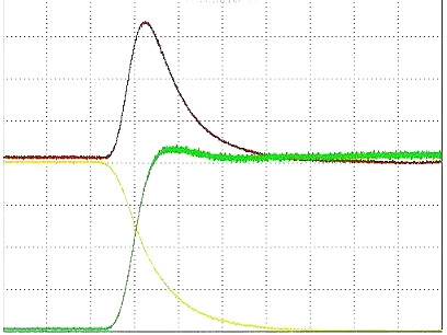
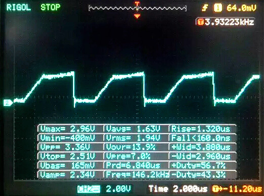
1、 Observing the G-pole waveform of the MOS transistor used with an oscilloscope, as shown in Figure 1, the rise time is close to 1.32us, and the fall time is close to<160ns (measured 50ns). Furthermore, referring to the manual shown in Figure 2, which requires the rise and fall edge of the MOS driver to be<35ns, and the fall time to be<80ns, it can be concluded that a long rise time leads to the MOS transistor working in a linear state, non switching state (see Summary 1). The long opening process of the MOS transistor directly leads to severe heating of the MOS transistor.
2、 Solution: Replace the driver current limiting resistor (Rg in Figure 2). Since there was no 4.99 ohm resistor in hand at the time, after replacing it with a 22 ohm resistor, the G-pole waveform is shown in Figure 3. Ton and Toff are close to the time required in Figure 2. When the MOS transistor is 24V, it carries a load of 27 ohms, with an output power of 21.3W and normal output voltage. The MOS transistor does not generate much heat.
Here is the solution to the problem:
1、 Observing the G-pole waveform of the MOS transistor used with an oscilloscope, as shown in Figure 1, the rise time is close to 1.32us, and the fall time is close to<160ns (measured 50ns). Furthermore, referring to the manual shown in Figure 2, which requires the rise and fall edge of the MOS driver to be<35ns, and the fall time to be<80ns, it can be concluded that a long rise time leads to the MOS transistor working in a linear state, non switching state (see Summary 1). The long opening process of the MOS transistor directly leads to severe heating of the MOS transistor.
2、 Solution: Replace the driver current limiting resistor (Rg in Figure 2). Since there was no 4.99 ohm resistor in hand at the time, after replacing it with a 22 ohm resistor, the G-pole waveform is shown in Figure 3. Ton and Toff are close to the time required in Figure 2. When the MOS transistor is 24V, it carries a load of 27 ohms, with an output power of 21.3W and normal output voltage. The MOS transistor does not generate much heat.
Summary 1: Summary of the causes of MOS tube heating
1. The problem with circuit design is to make the MOSFET work in a linear operating state, rather than in a switching state. This is also one of the reasons for the heating of MOS tubes. If N-MOS is used as a switch, the G-level voltage needs to be several volts higher than the power supply to fully conduct, while P-MOS is the opposite. Failure to fully open and excessive voltage drop leads to high success rate consumption, equivalent DC impedance is relatively high, voltage drop increases, so U * I also increases, and loss means heating. This is the most taboo mistake in designing circuits; (Although the problem points in this product testing are not related to circuit design, BOM errors are often more difficult to analyze than design errors.)
2. The frequency is too high, mainly due to the excessive pursuit of volume at times, which leads to an increase in frequency and an increase in losses on MOSFETs, resulting in an increase in heat generation;
3 . Insufficient heat dissipation design, high current, MOS transistor nominal current value, generally requires good heat dissipation to achieve. So if the ID is less than the maximum current, it may also generate severe heat and require sufficient auxiliary heat dissipation fins;
4. The selection of MOSFETs is incorrect, the power judgment is incorrect, and the internal resistance of MOSFETs is not fully considered, resulting in an increase in switch impedance
Summary 2: Analysis of the working status of MOSFETs
There are four working states of MOSFETs: on process, on state, off process, and off state;
The main losses of MOSFETs include switching loss, conduction loss, cutoff loss, as well as avalanche energy loss, switching
The loss is often greater than the latter;
The main causes of damage to MOSFETs are overcurrent (sustained high current or instantaneous high current), overvoltage (breakdown of D-S and G-S), and static electricity (which I personally believe can be classified as overvoltage);
Summary 3: Analysis of MOSFET Working Process
The working process of MOSFETs is very complex, with many variables inside. In short, slow switching is not easy to cause Miller oscillations (introducing Miller capacitors, Miller effects, etc. in detail), but switch losses will increase and heat generation will be high; The speed of the switch is fast, and the loss will be reduced, but Miller‘s oscillation is severe, which will actually increase the loss. The requirements for driving circuit wiring and main circuit wiring are very high, and the ultimate goal is to find a balance point. Generally, the opening process does not exceed 1us;
Summary 4: Important Parameters and Selection of MOSFETs
gs: When the gate is charged from 0V to the corresponding current Miller platform, the total charge is added, and at this time, Cgs is charged (equivalent to Ciss, input capacitor);
Qgd: The total charging charge of the entire Miller platform (not necessarily greater than Qgs, only referring to the Miller platform);
Qg: Total charging charge, including Qgs, Qgd, and others;
The unit of the above three parameters is nc (nanolibrary), usually ranging from a few nc to several tens of nc;
Rds (on): Conducting internal resistance, the smaller the loss under a certain voltage resistance;
General selection rules: tubes with smaller Qgs, Qgd, Qg, and Rds (on).
|
Disclaimer: This article is transferred from other platforms and does not represent the views and positions of this site. If there is any infringement or objection, please contact us to delete it. thank you! |


 Business consulting

 13823761625
 Mail me