


Conversion of 12 bit ADC analog signal to digital signal
Time:2024-03-28
Views:112
A 12 bit ADC is a progressive approximation type analog-to-digital converter. Its resolution can reach 12 bits. This means that it can convert analog signals into 12 bit binary numbers, with a numerical range between 0 and 4095.
The A/D conversion of each channel can be performed in single, continuous, scan, or intermittent modes. The conversion result can be stored in a 16 bit data register in a left aligned or right aligned manner. In addition, the 12 bit ADC also has an analog watchdog feature, allowing applications to detect whether the input voltage exceeds user-defined high/low thresholds. The input clock of ADC shall not exceed 14MHz, which is generated by dividing PCLK2.
It has up to 19 channels and can measure 16 external channels (16 analog inputs connected from external GPIO ports)
Three internal signal sources, namely internal temperature sensing (VSENSE) input, internal reference voltage (VREFINT) input, and external battery VBAT power supply pin input
The A/D conversion of each channel can be performed in single, continuous, scan, or intermittent modes.
The results of ADC can be stored in a 16 bit data register in either left aligned or right aligned manner.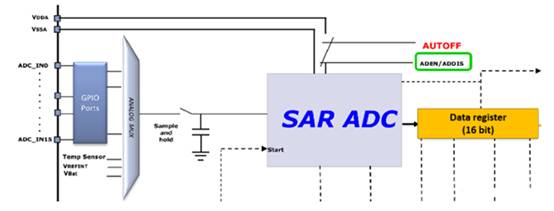 ADC characteristics
Range: The voltage range that can be measured is 0~3.6V
Resolution:
The resolution of an ADC is usually represented by the number of bits of the output binary number. The more bits there are, the higher the resolution. Generally speaking, the higher the resolution, the longer the conversion time.
Configurable conversion accuracy: 6 bits, 8 bits, 10 bits, 12 bits
Conversion time: The time required from the start of conversion to obtaining a stable digital output within the maximum allowable range of analog input voltage is called conversion time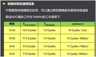 ADC workflow
The workflow of the ADC module can be divided into the following steps:
① Initialize ADC unit: including configuring clock, reference voltage source, sampling hold time, etc.
② Configure analog input channels and sampling time: Determine the analog input channels to be read and the sampling hold time.
③ Calibrate ADC unit: The ADC unit needs to be calibrated before each startup. The calibration process will automatically adjust the internal reference voltage to ensure accurate conversion.
④ Start ADC unit: Before the conversion, start the ADC unit through software to begin the conversion.
⑤ Read conversion result: After the conversion is completed, the ADC unit will trigger the conversion completion interrupt and store the conversion result in a register. At this point, the DMA channel can be used to transfer the conversion result to memory, or the value in the register can be directly read.
If continuous conversion is required for each channel, scanning mode can be used. The scanning mode allows for multiple conversions to be initiated at once and allows for setting the order of conversions.
The A/D conversion of each channel can be performed in single, continuous, scan, or intermittent modes. The conversion result can be stored in a 16 bit data register in a left aligned or right aligned manner. In addition, the 12 bit ADC also has an analog watchdog feature, allowing applications to detect whether the input voltage exceeds user-defined high/low thresholds. The input clock of ADC shall not exceed 14MHz, which is generated by dividing PCLK2.
It has up to 19 channels and can measure 16 external channels (16 analog inputs connected from external GPIO ports)
Three internal signal sources, namely internal temperature sensing (VSENSE) input, internal reference voltage (VREFINT) input, and external battery VBAT power supply pin input
The A/D conversion of each channel can be performed in single, continuous, scan, or intermittent modes.
The results of ADC can be stored in a 16 bit data register in either left aligned or right aligned manner.
Range: The voltage range that can be measured is 0~3.6V
Resolution:
The resolution of an ADC is usually represented by the number of bits of the output binary number. The more bits there are, the higher the resolution. Generally speaking, the higher the resolution, the longer the conversion time.
Configurable conversion accuracy: 6 bits, 8 bits, 10 bits, 12 bits
Conversion time: The time required from the start of conversion to obtaining a stable digital output within the maximum allowable range of analog input voltage is called conversion time
The workflow of the ADC module can be divided into the following steps:
① Initialize ADC unit: including configuring clock, reference voltage source, sampling hold time, etc.
② Configure analog input channels and sampling time: Determine the analog input channels to be read and the sampling hold time.
③ Calibrate ADC unit: The ADC unit needs to be calibrated before each startup. The calibration process will automatically adjust the internal reference voltage to ensure accurate conversion.
④ Start ADC unit: Before the conversion, start the ADC unit through software to begin the conversion.
⑤ Read conversion result: After the conversion is completed, the ADC unit will trigger the conversion completion interrupt and store the conversion result in a register. At this point, the DMA channel can be used to transfer the conversion result to memory, or the value in the register can be directly read.
If continuous conversion is required for each channel, scanning mode can be used. The scanning mode allows for multiple conversions to be initiated at once and allows for setting the order of conversions.
|
Disclaimer: This article is transferred from other platforms and does not represent the views and positions of this site. If there is any infringement or objection, please contact us to delete it. thank you! |


 Business consulting

 13823761625
 Mail me