


Can I take any value of DC-DC partial voltage feedback resistor?
Time:2024-04-02
Views:98
I believe that every hardware engineer should have used DC-DC, so have you ever thought about the value of the partial voltage feedback resistance?
In practical applications, the resistance value of the partial voltage resistance recommended in the manual is mostly copied directly, and even if there is no partial voltage resistance value corresponding to the output voltage, it is generally the resistance size close to the selection.
But there‘s always someone else who might have thought: i want to reduce the power consumption of the system, so I want to double the partial voltage resistance of FB, is there any risk?
 Recently, I saw a document in the folder of my computer that can answer this question, so I copied and pasted it directly, interested brothers can see that the main impact of the voltage divider resistance 4 aspects:
1. Efficiency
2, output voltage accuracy
3. Noise sensitivity
4. Stability
The full document is as follows:
introduction
Resistive voltage dividers are the most common network used in all DC/DC converter feedback systems. However, people often mistakenly think that it is a circuit that simply adjusts the output voltage by turning down the voltage to a certain reference voltage. After calculating the correct voltage divider ratio, the power designer must also be thoughtful when choosing the actual resistance values, because they will affect the overall performance of the converter.
This paper discusses some design considerations for resistive voltage dividers in feedback systems and the effects of such dividers on converter efficiency, output voltage accuracy, noise sensitivity, and stability.
1. Efficiency
witching DC/DC converters have relatively high efficiency because they operate through a number of low-loss components (e.g. Capacitors, inductors, and switches) provide power delivery to the load. High efficiency results in longer battery life, thus extending the operating time of portable devices.
or low-power DC/DC converters, a typical resistive feedback design requires a voltage divider resistor (R1+R2) with a very large total resistance (up to 1MΩ). This minimizes the current of the feedback divider. This current is applied to the load. Therefore, if the feedback divider resistance is small, the battery must provide more current and power for the same load. As a result, it is less efficient. This situation is not ideal, especially in some portable applications that require long battery life.
We have just discussed how to use large feedback resistors to improve efficiency. However, selecting too large a resistance will affect the output voltage accuracy of the converter. Because there is leakage current into the converter feedback pin.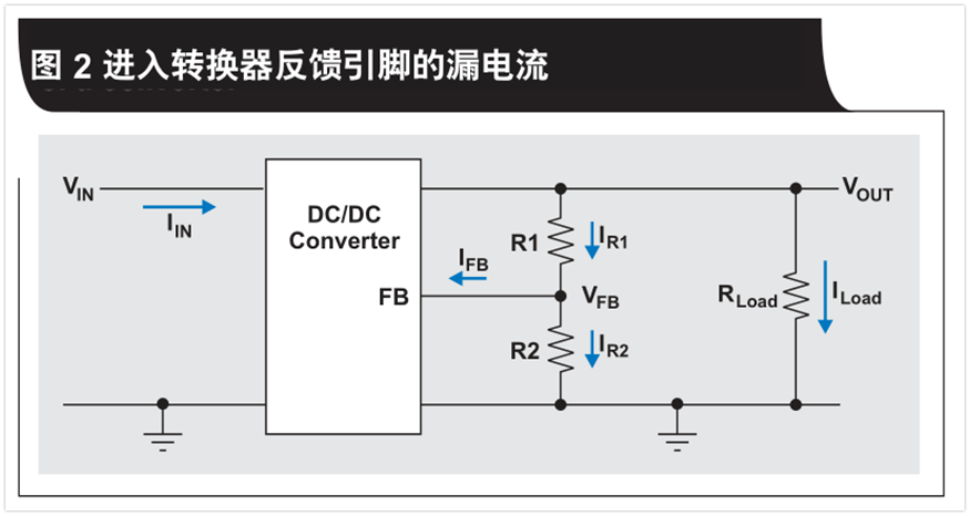 Figure 2 shows the current path of resistive feedback dividers (R1 and R2). When the feedback leakage current (IFB) is fixed, the current (lR1) of R1 decreases as the values of R1 and R2 increase. Thus, an increase in voltage divider resistance means a larger percentage of IR1 leakage current into the feedback pin, and a decrease in R2‘s current (1R2), resulting in a lower than expected feedback pin voltage (VFB). We set the output voltage by comparing the VFB with an internal reference voltage, so any error in the feedback voltage will result in an inaccurate output voltage. Equation 1 can be derived from Kirchhoff‘s current law. It shows that VFB is a function of R1 and R2:
 Please note that IFB is not fixed in real systems and varies from device to device and with operating conditions. To estimate the extreme change in output voltage due to leakage current, use the maximum specified value of IFB in the calculation. &, amp; , amp; , lt; , , , /span>
Design example 2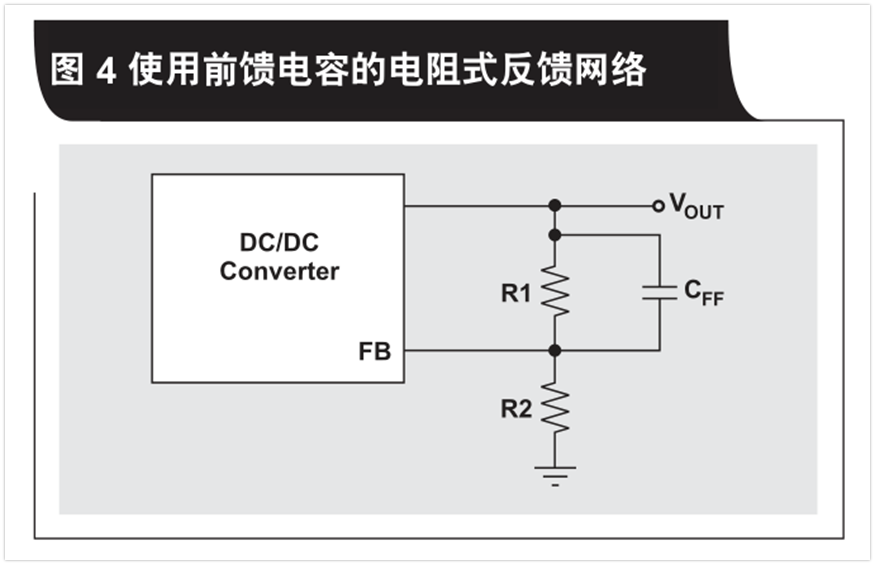


In practical applications, the resistance value of the partial voltage resistance recommended in the manual is mostly copied directly, and even if there is no partial voltage resistance value corresponding to the output voltage, it is generally the resistance size close to the selection.
But there‘s always someone else who might have thought: i want to reduce the power consumption of the system, so I want to double the partial voltage resistance of FB, is there any risk?
1. Efficiency
2, output voltage accuracy
3. Noise sensitivity
4. Stability
The full document is as follows:
introduction
Resistive voltage dividers are the most common network used in all DC/DC converter feedback systems. However, people often mistakenly think that it is a circuit that simply adjusts the output voltage by turning down the voltage to a certain reference voltage. After calculating the correct voltage divider ratio, the power designer must also be thoughtful when choosing the actual resistance values, because they will affect the overall performance of the converter.
This paper discusses some design considerations for resistive voltage dividers in feedback systems and the effects of such dividers on converter efficiency, output voltage accuracy, noise sensitivity, and stability.
1. Efficiency
witching DC/DC converters have relatively high efficiency because they operate through a number of low-loss components (e.g. Capacitors, inductors, and switches) provide power delivery to the load. High efficiency results in longer battery life, thus extending the operating time of portable devices.
or low-power DC/DC converters, a typical resistive feedback design requires a voltage divider resistor (R1+R2) with a very large total resistance (up to 1MΩ). This minimizes the current of the feedback divider. This current is applied to the load. Therefore, if the feedback divider resistance is small, the battery must provide more current and power for the same load. As a result, it is less efficient. This situation is not ideal, especially in some portable applications that require long battery life.
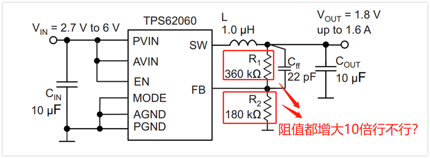
Design example 1
As Figure 1 shows, When the feedback resistance is low, the efficiency of the low load decreases. In this example, we use a (TI)TPS62060EVM with VIN =5V. VouT =1.8V and power saving mode enabled. At high load current, the load power consumption is much higher than that of resistive feedback network. This is why the efficiency of different R1 and R2 values is concentrated at high load currents. However, at low load current, the efficiency difference of different feedback resistors is more obvious. This is because the current of the divider dominates the current of the load. Therefore, in order to have a higher light load efficiency, a better design method is to use the large feedback resistance value suggested in the product specification sheet. If light load efficiency is not important in a particular design, smaller resistors can be used without significant impact on efficiency
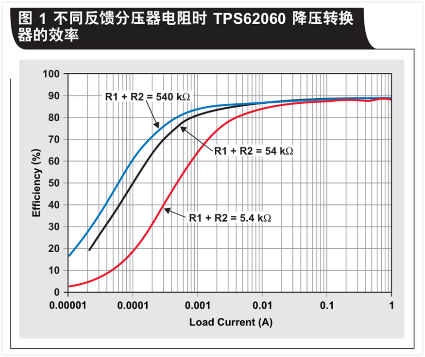
2, output voltage accuracyAs Figure 1 shows, When the feedback resistance is low, the efficiency of the low load decreases. In this example, we use a (TI)TPS62060EVM with VIN =5V. VouT =1.8V and power saving mode enabled. At high load current, the load power consumption is much higher than that of resistive feedback network. This is why the efficiency of different R1 and R2 values is concentrated at high load currents. However, at low load current, the efficiency difference of different feedback resistors is more obvious. This is because the current of the divider dominates the current of the load. Therefore, in order to have a higher light load efficiency, a better design method is to use the large feedback resistance value suggested in the product specification sheet. If light load efficiency is not important in a particular design, smaller resistors can be used without significant impact on efficiency
We have just discussed how to use large feedback resistors to improve efficiency. However, selecting too large a resistance will affect the output voltage accuracy of the converter. Because there is leakage current into the converter feedback pin.
Design example 2
Equation 1 and TI‘s TPS62130 buck converter are used to plot the feedback pin voltage and the corresponding output voltage as a function of the feedback divider resistance (see Figure 3). The voltage diagram is based on an ideal resistor that produces an output voltage of 3.3V and a feedback pin voltage of 0.8V. The only error term to be considered is the 100nA maximum feedback leakage current specified in the product specification.

Figure 3 shows that the feedback pin voltage decreases as the feedback divider resistance increases. Since the feedback pin voltage is compensated, the converter output is also compensated. At low resistance, there is no compensation for the feedback pin voltage, and the output is adjusted to the 3.3V specified in the design.
If the resistor R2 uses the recommended maximum of 400 kω (resulting in a total voltage resistance of 1650 kω), the leakage current produces only a small drop in output voltage. In general, the maximum value of the resistor specified in the product specification is to maintain the output voltage within the accuracy range specified in the product specification.
3. Noise sensitivity
Resistive voltage dividers are a noise source for converters. This noise, also known as thermal noise, increases when the voltage divider uses a large resistance value.
In addition, large resistance allows more noise to be coupled into the converter. There are many sources of this noise, including AM and FM radio waves, cell phone signals, and switching converters or RF transmitters on PCBS. Noise can even come from the switching DC/DC converter itself, especially if the PCB layout method is not correct. Since the resistive voltage divider is connected to a feedback pin, the closed-loop gain of the converter amplifies the noise, which appears at the output. To reduce sensitivity to other noise sources, designers can use smaller feedback resistors, better board layouts, or implement shielding. The use of small feedback resistors can indeed reduce noise sensitivity, but at the cost of slightly lower efficiency.
4, control loop, transient response and converter stability
Ideally, a stable converter should have a phase margin of at least 45° when measuring with a network analyzer. This large phase margin reduces or even eliminates output voltage ringing, thereby preventing damage to voltage-sensitive loads during input voltage transients or load transients.
Depending on the control topology, the product specification may require or recommend the use of feedforward capacitors (CFF) for resistive feedback networks. Figure 4 shows this device. Adding feedforward capacitors to resistive voltage dividers can generate zeros and poles, increase the converter‘s phase margin and cross frequency, and obtain a higher bandwidth and high stability system.
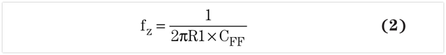
From the circuit transmission function shown in Figure 4, the zero fz and the pole fp are calculated using equations 2 and 3 respectively:
It is clear that both the zeros and poles are related to the values used by the resistance divider and the feedforward capacitance. Therefore, increasing or decreasing the resistance value to optimize efficiency, voltage accuracy, or noise changes the overall loop of the system. To maintain stability, you need to calculate a new CFF value using equation 4, based on the previous zero or the zero suggested in the product specification (whichever value is available, use it) :
Design example 3
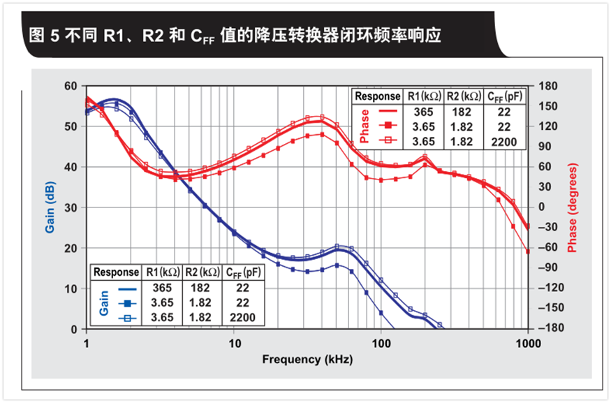
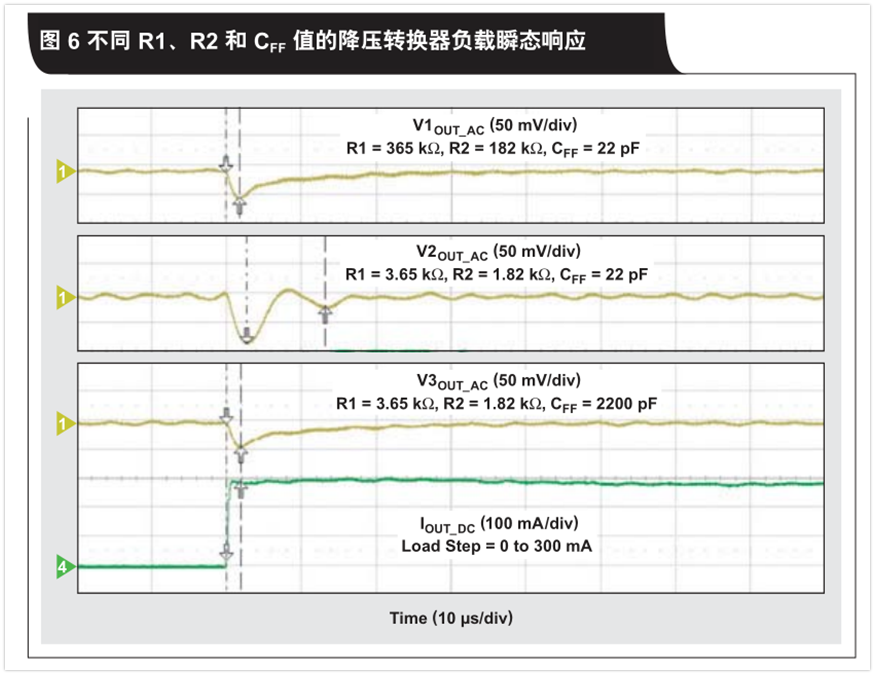
By using a buck converter, we see the effect of resistive voltage divider on the stability of the converter. In this example, we used the TI TPS62240 buck converter, and Vin=3.6V, Vout=1.8V, Lout=2.2uH, Cout=10uF, Iload=300mA.
By using a buck converter, we see the effect of resistive voltage divider on the stability of the converter. In this example, we used the TI TPS62240 buck converter, and Vin=3.6V, Vout=1.8V, Lout=2.2uH, Cout=10uF, Iload=300mA.
Figure 5 and Figure 6 show the closed-loop responses of three different resistive voltage divider networks and their corresponding transient responses, respectively. Each network uses a feedforward capacitor to describe how the divider network component changes the step-down converter stability. The converter is stable and the phase margin is 59° when using the recommended values in the product specification for the voltage divider network components (R1=365 kΩ, R2=182 kΩ and CFF =22pF). Its transient response verifies this, with a slight drop in output voltage and no oscillations.
When the feedback divider resistance is scaled down to R1=3.65kΩ and R2=1.82 kΩ, but the same feedforward capacitance CFF=22pF is used, the zeros and poles of the feedback network will change. The frequency response surface converter is less stable with a phase margin of 40°. The transient response of the converter demonstrates a larger output voltage drop and more ringing. In order to maintain the original frequency response and stability, we recalculate the CFF value for the new feedback resistance value.
Using equation 4, with a smaller resistance value and a feedforward capacitance of 2200pF, the new value can be calculated. The result is similar to the first case. The phase margin is 56°, the converter is stable, its transient response is verified, the output voltage drops slightly, and there is no oscillation.
For a converter that uses feedforward capacitors in its control topology, changing the value of the resistive divider makes it easy for the converter to steadily degrade. But this example merely shows that varying these values can maintain the same frequency response and transient response as long as the feedforward capacitance is properly adjusted.
Special case design
If the designer must use feedforward capacitors to improve stability, and the internal compensation of some converters requires a specific CFF value. In this case, equation 4 should not be used. Designers should use the suggested design equations in the product specification. For example, the TITPS61070 is internally compensated by a high side feedback resistor (R1). Its product specification suggests the following design equation for adding a capacitor in parallel with R1:
conclusion
Resistive feedback dividers or networks can affect the efficiency, output voltage accuracy, noise sensitivity, and stability of a DC/DC converter. In order to obtain the performance listed in the specific product specification, it is important to select the recommended value of the product specification for the feedback component. In addition, sometimes system requirements may deviate from these recommendations to meet other design goals. After understanding the advantages and disadvantages of these different parameters, designers can correctly select larger or smaller resistors to meet their application needs.
Resistive feedback dividers or networks can affect the efficiency, output voltage accuracy, noise sensitivity, and stability of a DC/DC converter. In order to obtain the performance listed in the specific product specification, it is important to select the recommended value of the product specification for the feedback component. In addition, sometimes system requirements may deviate from these recommendations to meet other design goals. After understanding the advantages and disadvantages of these different parameters, designers can correctly select larger or smaller resistors to meet their application needs.
|
Disclaimer: This article is transferred from other platforms and does not represent the views and positions of this site. If there is any infringement or objection, please contact us to delete it. thank you! |


 Business consulting

 13823761625
 Mail me