


Power Management Design Guidelines: Architecture, IC selection criteria
Time:2024-04-11
Views:89
Power management through a certain circuit topology, the different power input into the system to meet the needs of the output voltage. The Power supply directly affects the system performance, and the key component that determines the performance of the power supply is the Power Management Integrated Circuits (PMIC).
 The largest application field of PMIC is electronic consumer products, telecommunications, industrial control equipment, automotive terminals and other fields also have continuous demand for PMIC. All electronic devices have a power supply, but different systems have different requirements for power supply. In order to exert the performance of the electronic system, it is necessary to choose the appropriate power management mode.
1. Basic knowledge of power conversion
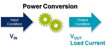
· Selecting the appropriate power management element depends on the input and output conditions of the application.
· Is the power input AC (AC) or DC (DC)?
· Is the input voltage higher or lower than the desired output voltage?
· What is the required load current?
· Is the load sensitive to noise, or requires constant current (as in LED applications), or is the current highly variable?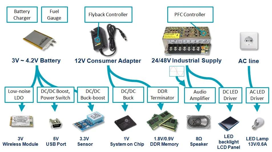 Different power conversion components are selected for each application based on its specific needs. The following figure shows several application examples and their typical commonly used power conversion components;
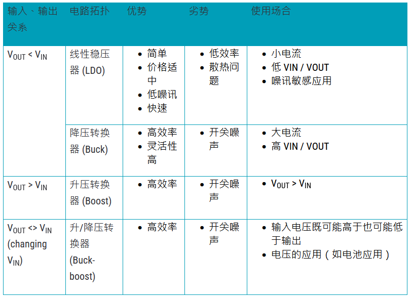
Figure 1. Application examples of power management
It is clear from the above examples that various parameters must be considered for optimal component selection. These parameters are described in detail below.
2. Selection standard of power management IC
When designing, the first consideration is the voltage difference between input and output (VIN-VOUT). When choosing the best power solution, the specific needs of the application, such as efficiency, heat dissipation limitations, noise, complexity and cost, must be considered.
Table 1. Basic criteria for the selection of low-voltage differential regulators, buck, boost, and boot-buck converters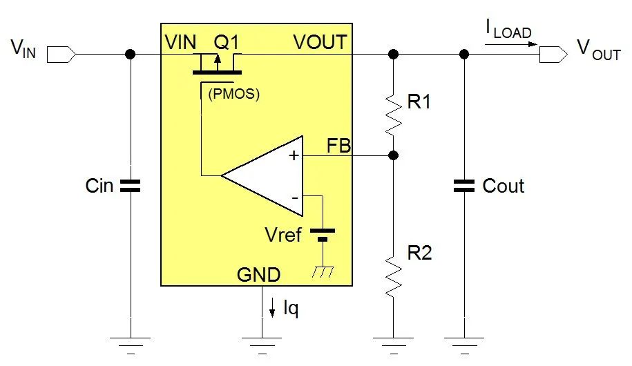 3. Review the main power architecture and power management components
When VOUT is less than VIN, the required output current and VIN/VOUT ratio are important factors to consider when choosing a low-voltage differential linear regulator (LDO) or Buck converter (Buck).
Low-voltage differential linear regulators (Ldos) are ideal for applications requiring low noise, low current, and low VIN/VOUT ratios. Its basic circuit diagram can be seen in Figure 2. The low-voltage differential linear regulator (LDO) regulates the output voltage by linearly controlling the on-off of the on-off element. Linear regulators provide accurate and noise-free output voltages that quickly respond to load changes at the output. However, linear regulation means that the voltage difference between the input and output multiplied by the average load current is the power consumed by the on-element of the linear regulator, i.e. Pd = (VIN-VOUT) * ILOAD. High VIN/VOUT ratios and high load currents can result in excessive additional power loss.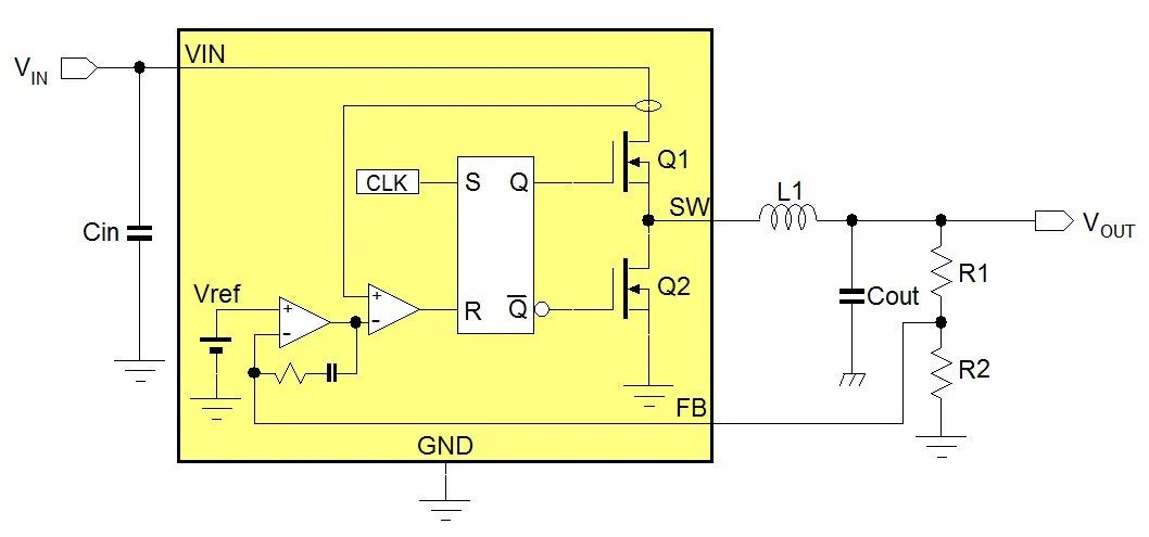
Figure 2. Schematic diagram of the basic circuit of low-voltage differential linear regulator (LDO)
Low-voltage differential linear regulators (Ldos) with high power consumption require a larger package size, which increases cost, PCB board space, and heat consumption. Therefore, when the LDO power consumption exceeds ~0.8W, it is more sensible to use buck converters as an alternative.
When selecting an LDO, the range of input and output voltages, the current size of the LDO, and the heat dissipation capacity of the package must be considered. The LDO voltage difference is the minimum voltage of VIN-VOUT within the adjustable range. In micro-power applications, where a single battery is needed for many years, the LDO static current IQ must be low enough to reduce unnecessary battery consumption. Such applications require special low-voltage differential linear regulators (LDO) with low static current IQ.
The buck converter is a switching buck converter that provides a high efficiency and high elasticity output at a high VIN/VOUT ratio and high load current. Its basic circuit is shown in Figure 3. Most buck converters consist of an internal high-side MOSFET and a low-side MOSFET that acts as a synchronous rectifier, alternating ON/OFF (ON/OFF) with an internal duty cycle control circuit to regulate the average output voltage. Noise caused by switching can be filtered by an external LC filter.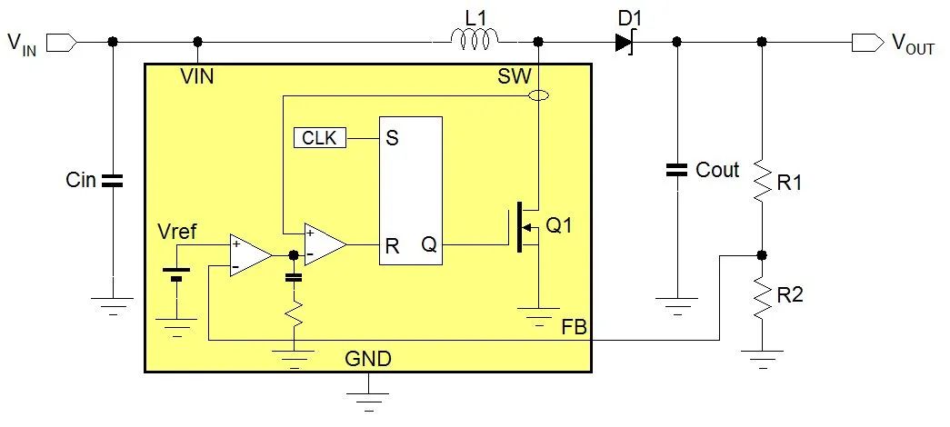
Figure 3. Basic circuit diagram of the converter
Because the two MOSFETs are alternating switches (ON or OFF), the power consumption is very small; By controlling the duty cycle, output with a large VIN/VOUT ratio can be produced. The on-resistance RDS(ON) of the internal MOSFET determines the current handling capability of the buck converter, while the rated voltage of the MOSFET determines the maximum input voltage. The switching frequency and the external LC filter element jointly determine the ripple voltage of the output. A buck converter with a higher switching frequency may use a smaller filter element, but the power consumption caused by switching will be increased. Step-down converters with pulse jump mode (PSM) reduce their switching frequency at light load, thereby improving efficiency at light load, which is important for applications requiring low power standby mode.
The boost converter is used for applications where VOUT is higher than VIN. The basic circuit diagram is shown in Figure 4. The boost converter increases the input voltage to a higher output voltage. The principle of operation is to charge the inductor through the internal MOSFET, and when the MOSFET is open, the inductor is discharged through the rectifier to the load end. Charging the inductor to discharging reverses the inductor voltage, raising the output voltage above the VIN. The ON/OFF duty ratio of the MOSFET switch will determine the boost ratio VOUT/VIN, and the feedback loop also controls the duty ratio to maintain a stable output voltage. The output capacitor is a buffer element used to reduce the output voltage continuous wave.
The MOSFET current absolute maximum rating and the boost ratio together determine the maximum load current, while the MOSFET voltage absolute maximum rating determines the maximum output voltage. Some boost converters will integrate the rectifier into the MOSFET to achieve synchronous rectification.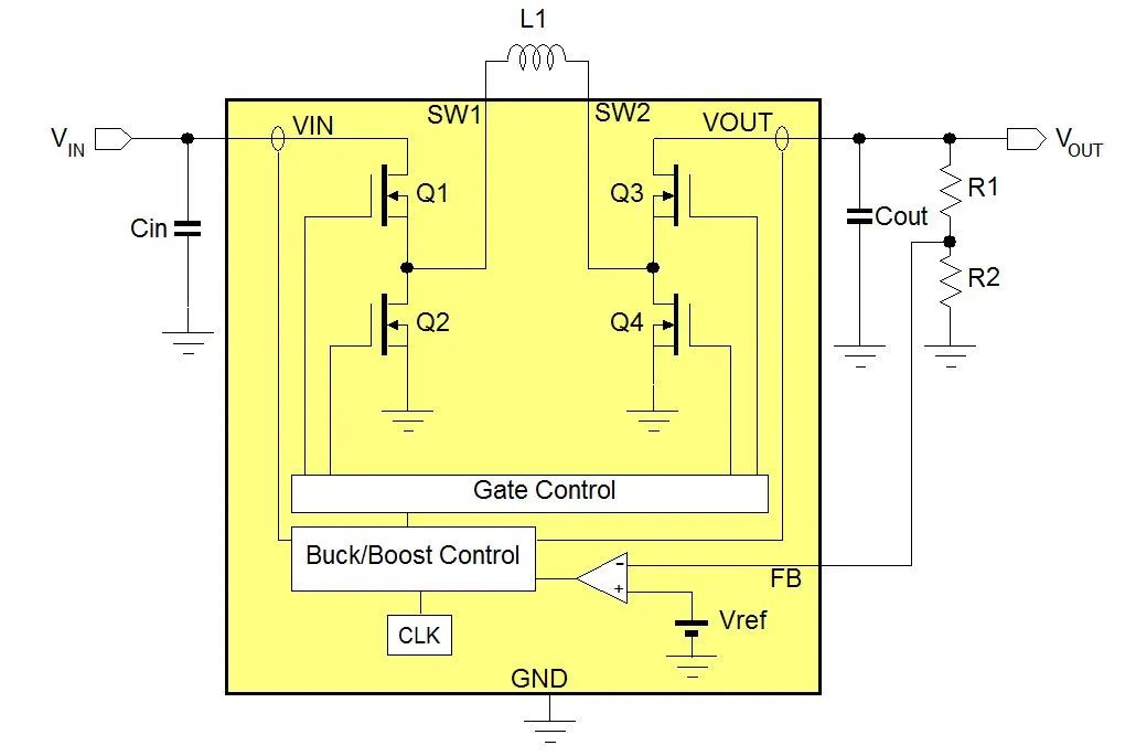
Figure 4. Schematic diagram of the basic circuit of the boost converter
Step-down converters are used in applications where the input voltage may change and can be lower or higher than the output voltage. In the booster to buck converter shown in Figure 5, the four internal MOSFET switches are automatically configured as buck converters when the VIN is higher than VOUT, and switch to boost operation mode when the VIN is lower than VOUT. This makes the up-buck converter ideal for battery-powered applications, especially when the battery voltage is lower than the regulated output voltage value to extend battery life. Because the four-switch up-buck converter is fully synchronized, it can achieve high efficiency. The output current capacity in buck mode is higher than that in boost mode. Because under the same load conditions, the boost mode and the buck mode compared, the former requires a higher switching current.
The absolute maximum voltage rating of the MOSFET will determine the maximum input and output voltage ranges. In applications where the output voltage does not require reference grounding, such as LED drivers, a booster to buck converter with only a single switch and rectifier can be used. And in most cases, the output voltage is referenced to the VIN.
Figure 5. A booster - buck converter with four internal switches
Most power management components use one of these four converter architectures.
Using internal or external MOSFETs?
Applications that require very large switching currents (e.g., >10A) often use an external switching MOSFETs, coupled with a step-down or step-up controller. This type of configuration is usually used in power converters with an output power of more than 25W.
Step-down applications with output current >25A mostly use a multi-phase step-down controller, that is, different phase stages share the same current. Circuits with very high switching voltages, such as those powered from AC line voltages, typically use an external, high-voltage MOSFETs as controllers.
The LED driver regulates the stable output current, not the stable output voltage, because the specific light output of the LED is completely determined by the current. The forward voltage of most high-brightness leds is 3 ~ 3.5V; Depending on the input voltage and the number of leds in the LED string, the converter can be buck, boost or booster.
LCD backlight systems must drive a large number of leds, so multi-string LED drivers are used. Some offline LED drivers use a linear LED driver architecture. Most LED drivers also include a dimming function so that they can control the output current and, in turn, the light output of the LED.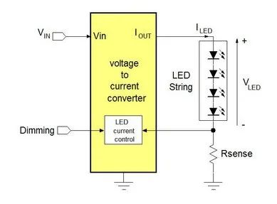
Figure 6. Basic circuit of LED driver
Protection function
Safety and reliability are of particular concern to power supplies. Most converters include protection that allows them to safely shut down the power supply in the event of excessive load or operating temperature.
The power switch can be used to control whether the power rail is connected to the circuit. Its basic circuit is shown in Figure 7.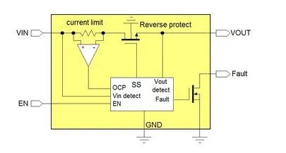
Figure 7. Power switches with different protection functions
The supplier‘s monitoring IC monitors the power supply for overvoltage or undervoltage. Figure 8 shows a typical power monitor detecting undervoltage.
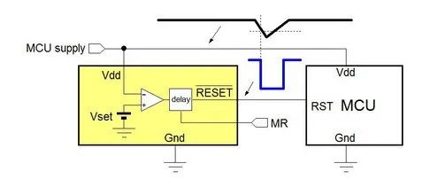
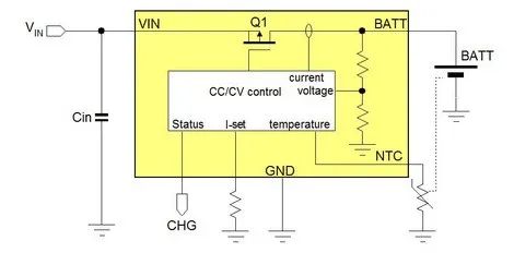
Figure 9. Basic circuit of linear battery charger
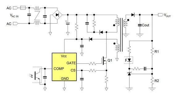
Figure 10. Basic AC/DC flyback power supply
1. Basic knowledge of power conversion
· Selecting the appropriate power management element depends on the input and output conditions of the application.
· Is the power input AC (AC) or DC (DC)?
· Is the input voltage higher or lower than the desired output voltage?
· What is the required load current?
· Is the load sensitive to noise, or requires constant current (as in LED applications), or is the current highly variable?
Figure 1. Application examples of power management
2. Selection standard of power management IC
When designing, the first consideration is the voltage difference between input and output (VIN-VOUT). When choosing the best power solution, the specific needs of the application, such as efficiency, heat dissipation limitations, noise, complexity and cost, must be considered.
Table 1. Basic criteria for the selection of low-voltage differential regulators, buck, boost, and boot-buck converters
When VOUT is less than VIN, the required output current and VIN/VOUT ratio are important factors to consider when choosing a low-voltage differential linear regulator (LDO) or Buck converter (Buck).
Low-voltage differential linear regulators (Ldos) are ideal for applications requiring low noise, low current, and low VIN/VOUT ratios. Its basic circuit diagram can be seen in Figure 2. The low-voltage differential linear regulator (LDO) regulates the output voltage by linearly controlling the on-off of the on-off element. Linear regulators provide accurate and noise-free output voltages that quickly respond to load changes at the output. However, linear regulation means that the voltage difference between the input and output multiplied by the average load current is the power consumed by the on-element of the linear regulator, i.e. Pd = (VIN-VOUT) * ILOAD. High VIN/VOUT ratios and high load currents can result in excessive additional power loss.
Figure 2. Schematic diagram of the basic circuit of low-voltage differential linear regulator (LDO)
When selecting an LDO, the range of input and output voltages, the current size of the LDO, and the heat dissipation capacity of the package must be considered. The LDO voltage difference is the minimum voltage of VIN-VOUT within the adjustable range. In micro-power applications, where a single battery is needed for many years, the LDO static current IQ must be low enough to reduce unnecessary battery consumption. Such applications require special low-voltage differential linear regulators (LDO) with low static current IQ.
The buck converter is a switching buck converter that provides a high efficiency and high elasticity output at a high VIN/VOUT ratio and high load current. Its basic circuit is shown in Figure 3. Most buck converters consist of an internal high-side MOSFET and a low-side MOSFET that acts as a synchronous rectifier, alternating ON/OFF (ON/OFF) with an internal duty cycle control circuit to regulate the average output voltage. Noise caused by switching can be filtered by an external LC filter.
Figure 3. Basic circuit diagram of the converter
The boost converter is used for applications where VOUT is higher than VIN. The basic circuit diagram is shown in Figure 4. The boost converter increases the input voltage to a higher output voltage. The principle of operation is to charge the inductor through the internal MOSFET, and when the MOSFET is open, the inductor is discharged through the rectifier to the load end. Charging the inductor to discharging reverses the inductor voltage, raising the output voltage above the VIN. The ON/OFF duty ratio of the MOSFET switch will determine the boost ratio VOUT/VIN, and the feedback loop also controls the duty ratio to maintain a stable output voltage. The output capacitor is a buffer element used to reduce the output voltage continuous wave.
The MOSFET current absolute maximum rating and the boost ratio together determine the maximum load current, while the MOSFET voltage absolute maximum rating determines the maximum output voltage. Some boost converters will integrate the rectifier into the MOSFET to achieve synchronous rectification.
Figure 4. Schematic diagram of the basic circuit of the boost converter
The absolute maximum voltage rating of the MOSFET will determine the maximum input and output voltage ranges. In applications where the output voltage does not require reference grounding, such as LED drivers, a booster to buck converter with only a single switch and rectifier can be used. And in most cases, the output voltage is referenced to the VIN.
Figure 5. A booster - buck converter with four internal switches
Using internal or external MOSFETs?
Applications that require very large switching currents (e.g., >10A) often use an external switching MOSFETs, coupled with a step-down or step-up controller. This type of configuration is usually used in power converters with an output power of more than 25W.
Step-down applications with output current >25A mostly use a multi-phase step-down controller, that is, different phase stages share the same current. Circuits with very high switching voltages, such as those powered from AC line voltages, typically use an external, high-voltage MOSFETs as controllers.
The LED driver regulates the stable output current, not the stable output voltage, because the specific light output of the LED is completely determined by the current. The forward voltage of most high-brightness leds is 3 ~ 3.5V; Depending on the input voltage and the number of leds in the LED string, the converter can be buck, boost or booster.
LCD backlight systems must drive a large number of leds, so multi-string LED drivers are used. Some offline LED drivers use a linear LED driver architecture. Most LED drivers also include a dimming function so that they can control the output current and, in turn, the light output of the LED.
Figure 6. Basic circuit of LED driver
Safety and reliability are of particular concern to power supplies. Most converters include protection that allows them to safely shut down the power supply in the event of excessive load or operating temperature.
The power switch can be used to control whether the power rail is connected to the circuit. Its basic circuit is shown in Figure 7.
Figure 7. Power switches with different protection functions
Figure 8. The power monitoring IC detects undervoltage of the power supply
The battery charger IC provides the correct charging current and voltage for the specific battery in the application.
Figure 9. Basic circuit of linear battery charger
AC/DC flyback controllers are used in applications where the AC line voltage needs to be converted into a stable, isolated supply voltage. Figure 10 shows a basic flyback power supply.
Figure 10. Basic AC/DC flyback power supply
Trends in power management
Bluetooth Low Energy, Wi-Fi 6 and Cellular iot are bringing connectivity to low-power iot devices. However, power management requires more than efficient chips, the electrical energy from the battery or power supply must also be regulated and distributed, and sometimes charged if the device is powered by a rechargeable battery. This means that no matter how efficient the processor, radio and memory in the wireless chip are, if the power management system is not optimized enough, it will affect battery life.
Building an efficient power management system is already a difficult task, but achieving a compact design is even more challenging. Space in many iot products is limited, but traditional power management solutions often consist of multiple chips, such as regulators, battery chargers, voltmeters, external watchdog and hard reset devices, which all take up valuable space.
Nordic solves both the efficiency and space challenges of power management with the nPM series power management IC (PMIC). The latest in the family, the nPM1300, features a high-precision coulometer that accurately measures the remaining battery power, extending the battery life of iot devices.
|
Disclaimer: This article is transferred from other platforms and does not represent the views and positions of this site. If there is any infringement or objection, please contact us to delete it. thank you! |


 Business consulting

 13823761625
 Mail me