


Touch MCU layout precautions
Time:2021-12-14
Views:2824
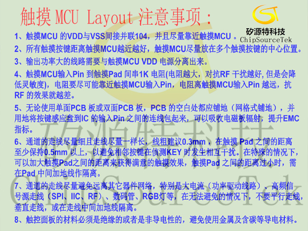
Touch MCU layout precautions:
1: VDD of touch MCU is indirectly connected in parallel with VSS 104 and as close to touch MCU as possible
2: The closer all touch keys are to touch MCU, the better. Touch MCU shall be placed in the center of multiple touch keys as far as possible
3: The circuit with high output power needs to be separated from the touch MCU VDD power supply
4: 1K resistance is connected between the touch MCU input pin and the touch pad (the greater the resistance, the better against RF interference, but the sensitivity will be reduced). The resistance should be as close to the touch MCU input pin as possible. The farther the resistance is from the touch MCU input pin, the worse the anti RF effect will be
5: Whether single-sided PCB board or double-sided PCB board is used, the blank piece of PCB shall be paved on the ground (in grid format) and wrapped with the connection between the ground pin key sensing disk and the input pin of IC, which can absorb the radiation of electromagnetic board and improve EMC index
6: The routing of the channel shall be as thin and as long as possible. The group thickness is recommended to be 0.3mm. The distance between touching pads can be protected at least 0.5mm to avoid mutual interference between adjacent keys when detecting keys Under special circumstances, the distance between touch pads can be increased to obtain satisfactory touch effect. If the distance between touch pads is too small, it is necessary to add ground wire in the middle of pad for isolation
7: The routing of the channel shall avoid being far away from other device networks as far as possible, especially high current (power drive line), high-frequency signal source routing (SPI, IIC, RF), nixie tube, RGB lamp, etc. in case of unavoidable, do not route in parallel, vertically, or add ground wire in the middle of the routing.
8: The material of the touch panel must be insulated or non-conductive, and avoid the use of conductive materials such as metal and carbon.
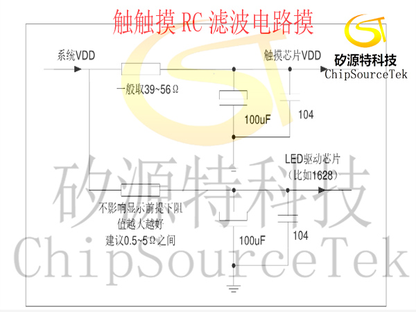
When the IC is working, the small change of voltage will affect the effect of touching the key. It is required that the ripple and noise of the power supply should be small. Attention should be paid to avoid external interference connected by the power supply, especially when applied to induction cooker and microwave oven. It must be able to effectively isolate external interference and voltage mutation. In the application with LED display, it is often easy to cause the fluctuation of power supply because of the instantaneous large current generated when scanning LED. Therefore, the RC filter circuit shown in the figure below is required between the system power supply and the touch chip (the marked parameters in the figure are typical recommended values). The more sensitive the touch key is, the smaller the ripple control is.
Typical application: when VDD = 5V, the ripple is controlled within 50mV when the sensitivity capacitance is 103, and within 20mV when the capacitance is 203.


 Business consulting

 13823761625
 Mail me