


NY8TM52D概述:
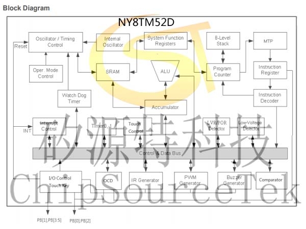
NY8TM52D是以MTP作為程式記憶體的8位元微控制器,適合IO產品的應用。而MTP作為程式記憶體能更方便且有效率的開發產品。NY8TM52D核心建立在RISC精簡指令集架構可以很容易地做編輯和控制,共有55條指令。除了少數指令需要2個時序,大多數指令都是1個時序即能完成,可以讓使用者輕鬆地以程式控制完成不同的應用。因此非常適合各種中低記憶容量但又複雜的應用。
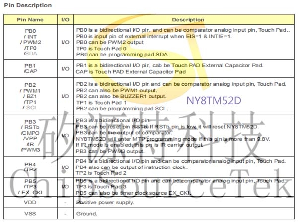
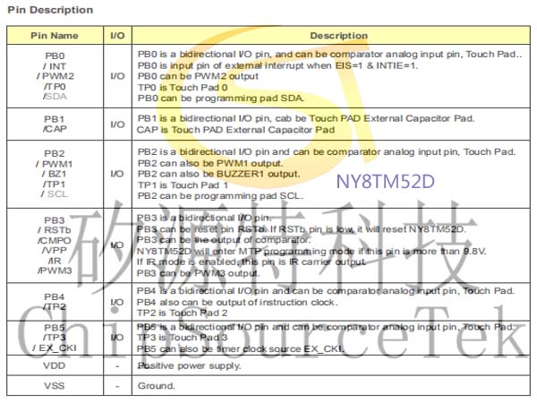
NY8TM52D有6根彈性的雙向I/O腳,每個I/O腳都有單獨的暫存器控制為輸入或輸出腳。而且每一個I/O腳位都有附加的程式控制功能如上拉或下拉電阻或開漏極(Open-Drain) 輸出。此外針對紅外線搖控的產品方面,NY8TM52D內建了可選擇頻率的紅外載波發射口。其中有4根I/O具備觸控開關功能,可經由暫存器控制為觸控開關輸入腳位。NY8TM52D內建電壓比較器,亦可藉由暫存器選擇I/O當電壓輸入與比較結果輸出。
NY8TM52D有兩組計時器,可用系統頻率當作一般的計時的應用或者從外部訊號觸發來計數。另外NY8TM52D提供3組10位元解析度的PWM輸出及一組蜂鳴器輸出,可用來驅動馬達、LED、或蜂鳴器等等。
NY8TM52D採用雙時鐘機制,高速振盪或者低速振盪都由內部RC振盪輸入。在雙時鐘機制下,NY8TM52D可選擇多種工作模式如正常模式(Normal)、慢速模式(Slow mode)、待機模式(Standby mode) 與睡眠模式(Halt mode)可節省電力消耗延長電池壽命。
在省電的模式下如待機模式(Standby mode)與睡眠模式(Halt mode)中,有多種事件可以觸發中斷喚醒NY8TM52D進入正常操作模式(Normal) 或 慢速模式(Slow mode) 來處理突發事件。
NY8TM52D功能:
寬廣的工作電壓:
2.4V ~ 5.5V @系統頻率≦8MHz。
3.0V ~ 5.5V @系統頻率>8MHz。
寬廣的工作温度:-40°C ~ 85°C。
2Kx14 bits MTP。
128 bytes SRAM。
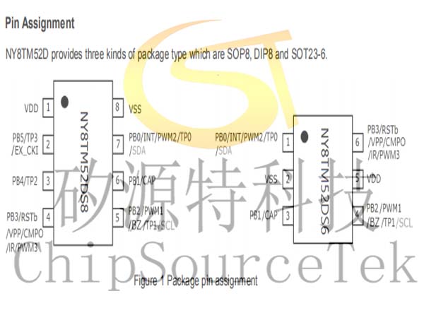
6根可分別單獨控制輸入輸出方向的I/O腳(GPIO)、PB[5:0]。
PB[3:0]可選擇輸入時使用內建下拉電阻。
PB[5:0]可選擇上拉電阻或開漏極輸出(Open-Drain)。
8層程式堆棧(Stack)。
存取資料有直接或間接定址模式。
一組8位元上數計時器(Timer0)包含可程式化的頻率預除線路。
一組10位元下數計時器(Timer1)可選重複載入或連續下數計時。
三個10位元的脈衝寬度調變輸出(PWM1/2/3)。
一個蜂鳴器輸出(BZ1)。
38/57KHz紅外線載波頻率可供選擇,同時載波之極性也可以根據數據作選擇。
內建上電復位電路(POR)。
內建低壓復位功能(LVR)。
內建16.段低電壓偵測功能(LVD)。
內建準確的電壓比較器(Voltage Comparator)。
內建4鍵觸控輸入腳
內建看門狗計時(WDT),可由程式韌體控制開關。
雙時鐘機制,系統可以隨時切換高速振盪或者低速振盪。
高速振盪: I_HRC (1~20MHz內部高速RC振盪)
低速振盪: I_LRC (內部 32KHz低速RC振盪)
四種工作模式可隨系統需求調整電流消耗:正常模式(Normal)、慢速模式(Slow mode)、待機模式(Standby mode) 與睡眠模式(Halt mode)。
八種硬體中斷:
Timer0 溢位中斷。
Timer1 借位中斷。
WDT 中斷。
PB 輸入狀態改變中斷。
外部中斷輸入。
低電壓偵測中斷。
觸控比較器中斷。
觸控計數器溢位中斷。
NY8TM52D在待機模式(Standby mode)下的八種喚醒中斷:
Timer0 溢位中斷。
Timer1 借位中斷。
WDT 中斷。
PB 輸入狀態改變中斷。
外部中斷輸入。
低電壓偵測中斷。
觸控比較器中斷。
觸控計數器溢位中斷。
NY8TM52D在睡眠模式(Halt mode)下的五種喚醒中斷:
WDT 中斷。
PB 輸入狀態改變中斷。
外部中斷輸入。
觸控比較器中斷。
觸控計數器溢位中斷。
NY8TM52D提供兩種電流檔位(Normal/Large)
NY8TM52D Block Diagram:

NY8TM52D .
Pin Assignment
NY8TM52D provides three kinds of package type which are SOP8, DIP8 and SOT23-6.
NY8TM52D Pin Description:
Memory Organization:
NY8TM52D memory is divided into two categories: one is program memory and the other is data memory. Data memory is sub-divided into SRAM/Register Memory.
Program Memory:NY8TM52D Pin Description:
Memory Organization:
NY8TM52D memory is divided into two categories: one is program memory and the other is data memory. Data memory is sub-divided into SRAM/Register Memory.
The program memory space of NY8TM52D is 2K words. Therefore, the Program Counter (PC) is 11-bit wide in order to address any location of program memory.
Some locations of program memory are reserved as interrupt entrance. Power-On Reset vector is located at 0x000. Software interrupt vector is located at 0x001. Internal and external hardware interrupt vector is located at 0x008.
NY8TM52D provides instruction GOTOA, CALLA to address 256 location of program space. NY8TM52D also provides instructions LCALL and LGOTO to address any location of program space.
When a call or interrupt is happening, next ROM address is written to top of the stack, when RET, RETIA or RETIE instruction is executed, the top of stack data is read and load to PC.
NY8TM52D program ROM address 0x7FE~0x7FF are reserved space, if user tries to write code in these addresses will get unexpected false functions.
NY8TM52D program ROM address 0x00E~0x00F are preset rolling code can be released and used as normal program space.
SRAM/Register Memory
According to instructions used to access SRAM/register memory, the memory can be divided into three kinds of categories: one is R-page Special-function Register (SFR) + General Purpose Register (GPR), another is F-page SFR, the others are S-page SFR and T-page SFR. GPR are made of SRAM and user can use them to store variables or intermediate results.
R-page data memory is divided into 4 banks and can be accessed directly or indirectly through a SFR register which is File Select Register (FSR). STATUS[7:6] are used as Bank register BK[1:0] to select one bank out of the 4 banks.
R-page register can be divided into addressing mode: direct addressing mode and indirect addressing mode. The indirect addressing mode of data memory access is described in the following graph. This indirect addressing mode is implied by accessing register INDF. The bank selection is determined by STATUS[7:6] and the location selection is from FSR[6:0].


 发送邮件
发送邮件 商务QQ客服
 13823761625

