


X-FAB introduces image sensor backlighting technology to enhance CMOS sensor performance
Time:2024-04-19
Views:74
Source: X-FAB Author: X-FAB
Beijing, China, April 9, 2024 - X-FAB Silicon Foundries (" X-FAB "), a globally recognized analog/mixed-signal foundry of excellence, today announced the addition of a new member to its optical sensor product platform - to meet the performance requirements of a new generation of image sensors. X-FAB has now enabled backlighting (BSI) on its popular CMOS sensor process platform XS018 (180 nm).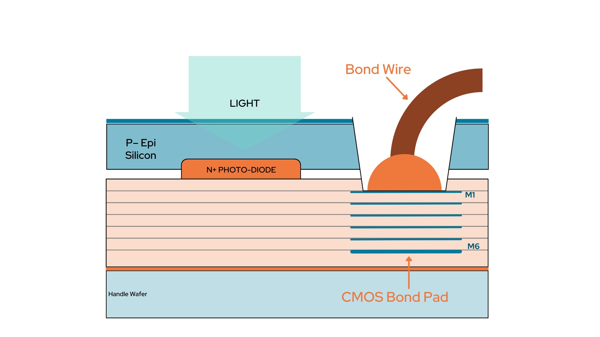
BSI process cross-section diagram
Through the BSI process, the performance of image sensitive pixels will be greatly enhanced. This technology allows the incident light received by each pixel to no longer be blocked by the metal layer of the back-end process, greatly improving the sensor fill ratio up to 100%. Due to its ability to obtain higher pixel sensitivity, this advantage is particularly significant in low light conditions. At the same time, due to the shortening of the light path, the BSI process can also effectively reduce the crosstalk between adjacent pixels, thereby improving the image quality. Although the current BSI technology has been widely used in 300 mm wafers, and widely used in consumer small pixel image sensors, but for the 200 mm wafer market, mainly used in industrial medical vehicles and other fields; Or for large pixel image sensors that need to be stitched together, especially in scenarios that require additional customization, the choice of BSI processes on the market is very limited. As a result, X-FAB has added BSI capabilities to its acclaimed CMOS sensor process platform XS018, opening up new possibilities for different market segments: whether X-ray diagnostic equipment, industrial automation systems, astronomical research, robot navigation, in-vehicle front-facing cameras, or more, customers can easily meet the most demanding application requirements.
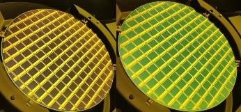
BSI process and standard visible light anti-reflection layer (left), wafer using BSI process and near infrared anti-reflection layer (right)
The XS018 CMOS sensor platform is characterized by fast readout speed and low dark current, and customers can also select a variety of different epitaxial layer thickens on the platform to realize image sensors for different application scenarios. In addition, through the BSI process, customers have the option to add ARC layers, which can be adjusted to meet different special application requirements. The included X-FAB Design support package covers the complete workflow from initial design to shipment of engineering samples, including a complete PDK.
BSI technology can position the sensor closer to the light source and avoid unnecessary circuit obstacles to improve image imaging capabilities, so it is increasingly used in modern imaging devices. This has proven to be very useful in low-light environments." Heming Wei, X-FAB‘s optical sensor Technology Marketing Manager, said, "Although such applications were previously focused on the consumer electronics sector, there is now a lot of demand in the industrial, automotive and medical markets. "With X-FAB‘s BSI process, we can combine the advantages of higher sensitivity, larger sensor size and pixel capacity to deliver market-convincing products that meet the needs of industrial, automotive and medical applications."
Abbreviations:
ARC anti-reflection coating
BSI backlight technology
CMOS complementary metal oxide semiconductor
PDK process design kit
Beijing, China, April 9, 2024 - X-FAB Silicon Foundries (" X-FAB "), a globally recognized analog/mixed-signal foundry of excellence, today announced the addition of a new member to its optical sensor product platform - to meet the performance requirements of a new generation of image sensors. X-FAB has now enabled backlighting (BSI) on its popular CMOS sensor process platform XS018 (180 nm).
BSI process cross-section diagram
BSI process and standard visible light anti-reflection layer (left), wafer using BSI process and near infrared anti-reflection layer (right)
BSI technology can position the sensor closer to the light source and avoid unnecessary circuit obstacles to improve image imaging capabilities, so it is increasingly used in modern imaging devices. This has proven to be very useful in low-light environments." Heming Wei, X-FAB‘s optical sensor Technology Marketing Manager, said, "Although such applications were previously focused on the consumer electronics sector, there is now a lot of demand in the industrial, automotive and medical markets. "With X-FAB‘s BSI process, we can combine the advantages of higher sensitivity, larger sensor size and pixel capacity to deliver market-convincing products that meet the needs of industrial, automotive and medical applications."
Abbreviations:
ARC anti-reflection coating
BSI backlight technology
CMOS complementary metal oxide semiconductor
PDK process design kit
# # #
About X-FAB:
X-FAB is a leading analog/mixed-signal and MEMS foundry group that produces silicon wafers for automotive, industrial, consumer, medical and other applications. Using modular CMOS and SOI processes ranging in size from 1.0μm to 110nm, and featuring SiC and micro-electro-mechanical systems (MEMS) long life processes, X-FAB delivers the highest quality standards, manufacturing excellence and innovative solutions to customers worldwide. X-FAB‘s analog digital integrated circuits (mixed-signal ics), sensor MEMS are manufactured at six manufacturing sites in Germany, France, Malaysia and the United States, and employs approximately 4,200 people worldwide. www.xfab.com
X-FAB is a leading analog/mixed-signal and MEMS foundry group that produces silicon wafers for automotive, industrial, consumer, medical and other applications. Using modular CMOS and SOI processes ranging in size from 1.0μm to 110nm, and featuring SiC and micro-electro-mechanical systems (MEMS) long life processes, X-FAB delivers the highest quality standards, manufacturing excellence and innovative solutions to customers worldwide. X-FAB‘s analog digital integrated circuits (mixed-signal ics), sensor MEMS are manufactured at six manufacturing sites in Germany, France, Malaysia and the United States, and employs approximately 4,200 people worldwide. www.xfab.com
|
Disclaimer: This article is transferred from other platforms and does not represent the views and positions of this site. If there is any infringement or objection, please contact us to delete it. thank you! |


 Business consulting

 13823761625
 Mail me