


NY8TM52D General Description:
NY8TM52D is a touchable MCU.
NY8TM52D is a MTP based 8-bit MCU tailored for I/O based applications like remote controllers, fan/light controller, game controllers, toy and various controllers. The MTP offers the advantage of convenient and effective way of developing user program. NY8TM52D adopts advanced CMOS technology to provide customers remarkable solution with low cost and high performance benefits. RISC architecture is applied to NY8TM52D and it provides 55 instructions. All instructions are executed in single instruction cycle except program branch and skip instructions which will take two instruction cycles. Therefore, NY8TM52D is very suitable for those applications that are sophisticated but compact program size is required.
NY8TM52D provide on-chip debug (OCD) facilities as a low cost alternative to ICE. With OCD and a minimum of extra hardware, NY8TM52D can do ICE tasks such as free running, single stepping, break point setting and internal ram/register accessing.
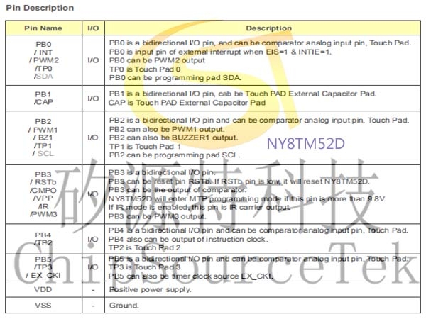
As NY8TM52D address I/O type applications, it can provide 6 I/O pins for applications which require abundant input and output functionality. Moreover, each I/O pin may have additional features, like Pull-High/Pull-Low resistor and open-drain output type through programming. Moreover, NY8TM52D has built-in infrared (IR) carrier generator with selectable IR carrier frequency and polarity for applications which demand remote control feature. Multiple Touch-Keys is from 1 touch key up to 4 touch keys configured by register option. A built-in LDO regulator for touch sensor can provide a stable capacitive sensing design for touch application. An innovative software tool “Q-Touch” is provided to develop the different touch applications
NY8TM52D also provides 2 sets of timers which can be used as regular timer based on system oscillation or event counter with external trigger clock. Moreover, NY8TM52D provides 3 set of 10-bit resolution Pulse Width Modulation (PWM1/2/3) output and 1 set buzzer output in order to drive motor/LED and buzzer.
NY8TM52D employs dual-clock oscillation mechanism, both high oscillation or low oscillation can be derived from internal resistor/capacitor oscillator. Moreover, based on dual-clock mechanism, NY8TM52D provides kinds of operation mode like Normal mode, Slow mode, Standby mode and Halt mode in order to save power consumption and lengthen battery operation life.
While NY8TM52D operates in Standby mode and Halt mode, kinds of event will issue interrupt requests and can wake-up NY8TM52D to enter Normal mode and Slow mode in order to process urgent events.
NY8TM52D Features:
NY8TM52D Features:
Wide operating voltage range:
2.4V ~ 5.5V @system clock ≦8MHz.
3.0V ~ 5.5V @system clock >8MHz.
Wide operating temperature: -40°C ~ 85°C.
2K x 14 bits MTP. ? 128 bytes SRAM.
6 general purpose I/O pins (GPIO), PB[5:0], with independent direction control.
PB[3:0] have features of Pull-Low resistor for input pin.
PB[5:0] have features of Pull-High resistor, and open-drain output.
8-level hardware Stack.
Direct and indirect addressing modes for data access.
One 8-bit up-count timer (Timer0) with programmable prescaler.
One 10-bit reload or continuous down-count timers (Timer1).
Three 10-bit resolution PWM (PWM1/2/3) output.
One buzzer (BZ1) output.
Selectable 38/57KHz IR carrier frequency and high/low polarity according to data value.
Built-in Power-On Reset (POR).
Built-in high-precision Low-voltage detector(LVD) .
Built-in high-precision Voltage Comparator.
Built-in 4-key Touch pad
Built-in Low-Voltage Reset (LVR).
Built-in 16-segment Low-Voltage Detect (LVD).
Built-in Watch-Dog Timer (WDT) enabled/disabled by firmware control.
Dual-clock oscillation: System clock can switch between high oscillation and low oscillation.
High oscillation: I_HRC (Internal High Resistor/Capacitor Oscillator ranging from 1M~20MHz) ? Low oscillation: I_LRC (Internal 32KHz oscillator)
Four kinds of operation mode to reduce system power consumption:
Normal mode, Slow mode, Standby mode and Halt mode.
Eight hardware interrupt events: ? Timer0 overflow interrupt.
Timer1 underflow interrupt.
WDT timeout interrupt.
PB input change interrupt.
External interrupt.
LVD interrupt.
Touch comparator interrupt
Touch counter overflow interrupt
Eight interrupt events to wake-up NY8TM52D from Standby mode:
Timer0 overflow interrupt.
Timer1 underflow interrupt.

NY8TM52D .
WDT timeout interrupt.
PB input change interrupt.
External interrupt.
LVD interrupt.
Touch comparator interrupt
Touch counter overflow interrupt
Five interrupt events to wake-up NY8TM52D from Halt mode: ? WDT timeout interrupt.
PB input change interrupt.
External interrupt.
Touch comparator interrupt
Touch counter overflow interrupt
There are two current options (Normal/Large) can be selected.
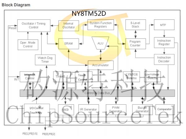
NY8TM52D Block Diagram:
NY8TM52D Block Diagram:
NY8TM52D .
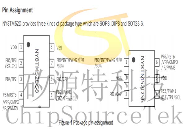
Pin Assignment
NY8TM52D provides three kinds of package type which are SOP8, DIP8 and SOT23-6.
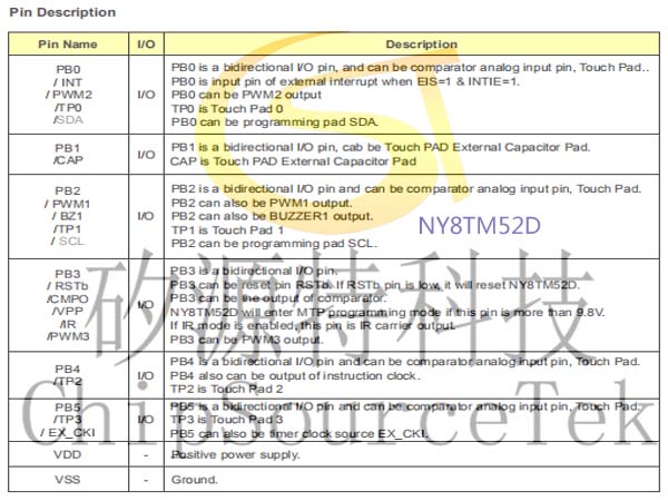
NY8TM52D Pin Description:
Memory Organization:
NY8TM52D memory is divided into two categories: one is program memory and the other is data memory. Data memory is sub-divided into SRAM/Register Memory.
Program Memory:NY8TM52D Pin Description:
Memory Organization:
NY8TM52D memory is divided into two categories: one is program memory and the other is data memory. Data memory is sub-divided into SRAM/Register Memory.
The program memory space of NY8TM52D is 2K words. Therefore, the Program Counter (PC) is 11-bit wide in order to address any location of program memory.
Some locations of program memory are reserved as interrupt entrance. Power-On Reset vector is located at 0x000. Software interrupt vector is located at 0x001. Internal and external hardware interrupt vector is located at 0x008.
NY8TM52D provides instruction GOTOA, CALLA to address 256 location of program space. NY8TM52D also provides instructions LCALL and LGOTO to address any location of program space.
When a call or interrupt is happening, next ROM address is written to top of the stack, when RET, RETIA or RETIE instruction is executed, the top of stack data is read and load to PC.
NY8TM52D program ROM address 0x7FE~0x7FF are reserved space, if user tries to write code in these addresses will get unexpected false functions.
NY8TM52D program ROM address 0x00E~0x00F are preset rolling code can be released and used as normal program space.
SRAM/Register Memory
According to instructions used to access SRAM/register memory, the memory can be divided into three kinds of categories: one is R-page Special-function Register (SFR) + General Purpose Register (GPR), another is F-page SFR, the others are S-page SFR and T-page SFR. GPR are made of SRAM and user can use them to store variables or intermediate results.
R-page data memory is divided into 4 banks and can be accessed directly or indirectly through a SFR register which is File Select Register (FSR). STATUS[7:6] are used as Bank register BK[1:0] to select one bank out of the 4 banks.
R-page register can be divided into addressing mode: direct addressing mode and indirect addressing mode. The indirect addressing mode of data memory access is described in the following graph. This indirect addressing mode is implied by accessing register INDF. The bank selection is determined by STATUS[7:6] and the location selection is from FSR[6:0].


 Business consulting

 13823761625
 Mail me