


CST5040A/5041S1 General Descriptions:
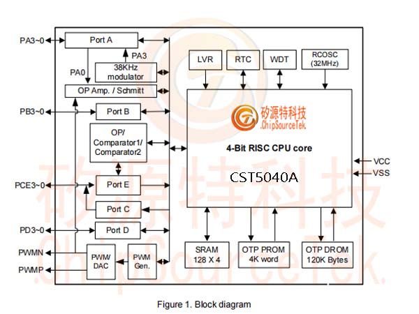
CST5040A/5041S1 series are 4-bits micro-controller which could play 4 channel melody or 4 channel ADPCM with PWM direct drive circuit. PWM resolution is 8/10/12 bits. They include a low cost, high performance CMOS micro-processor. The clock frequency of this up is typically 8.192 (±3%) MHz. This chip operates over a wide voltage range of 2.0V~5.5V. It contains program ROM (PROM) and data ROM (DROM) inside. The maximum program ROM is 4K words and maximum data ROM size is 120K byte. The maximum working SRAM is (128+2) nibbles. It is provided with total 16 software programmable I/O Ports.
CST5040A/5041S1 Features:
Operating voltage: 2.0V to 5.5V
MCU Operation frequency: 8.192MHz
Memory Size
Program ROM size: 4K*12-bits OTP type
Data ROM size: Maximum 120K*8-bits OTP type
SRAM size: 128*4 bits
User register: 2*4 bits
Wakeup function for power-down mode:
HALT mode wakeup source: Port A, Port B, Port D and Port E/CE can wake-up from HALT mode to
NORMAL mode and executing wake-up sub-routine program.
RTC wakeup: Clock source comes from internal LRCOSC, time period 1/16/64/128 ms.
RTC wakeup function only support in CST5041S1.
12 input/output pins: Port A, Port B and Port D can be defined as input or output port bit by bit.
4 input/output ports or 4 input only ports or 4 output only ports “Port CE/E/C” defined by option:
If input only ports are employed, Port E defined as input only ports.
If output only ports are employed, Port C defined as output only ports.
If input/output ports are selected, Port CE defined as input/output ports bit by bit.
Four reset condition:
Low voltage reset. (LVR = 2.0V)
Power on reset.
External reset pin. (active low)
Watch dog timer overflow.
One internal interrupt sources:
PWM interrupt.
WDT
Watch dog timer, can enabled/disabled by option.
WDT period is 256*256*16/Fsys. (WDT period is 0.13 sec for system clock=8.192MHz)
Audio output:
Support PWM or DAC mode by option.
Support 8/10/12 bits.
Support option set for pull down resistor 1M, 50K or 220K Ohm, reset pin (PB3 or PC3), low voltage reset…etc.
Oscillator fuse option ±3%, temperature & voltage compensation.
Support security option (1 bit) for read inhibition.
Support 16-levels LVD function.
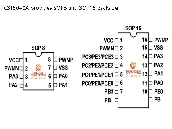
CST5040A provides SOP8 and SOP16 package:

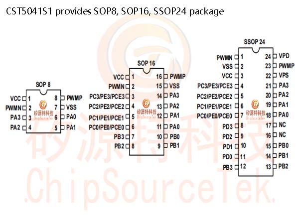
CST5041S1 provides SOP8, SOP16, SSOP24 package:
CST5040A/5041S1 Block Diagram:
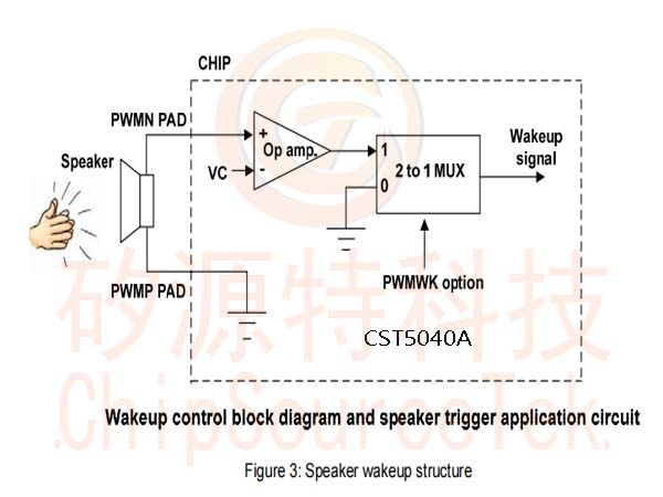
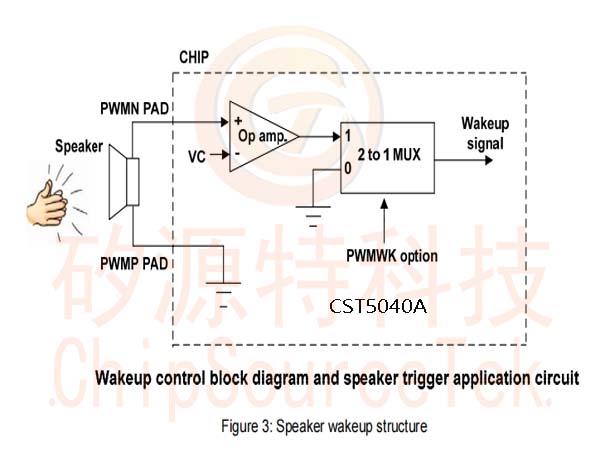
CST5040A/5041S1 Speaker wakeup structure:
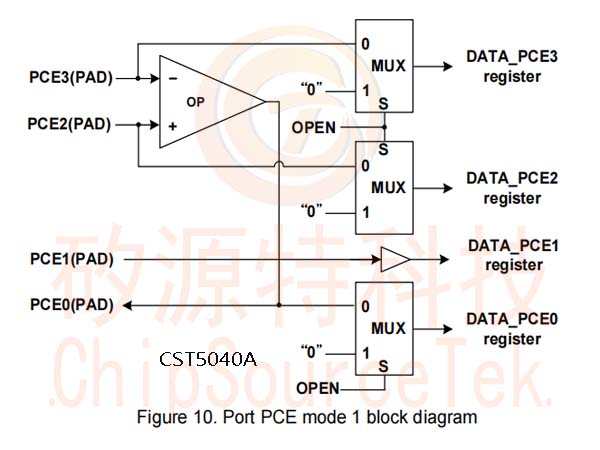
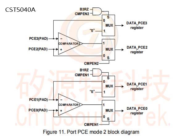
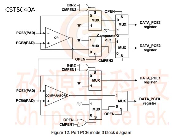
CST5040A/5041S1 Port PCE mode block diagram:
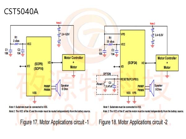
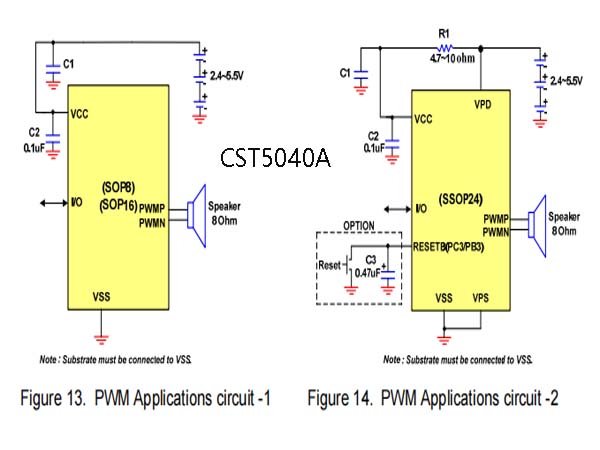
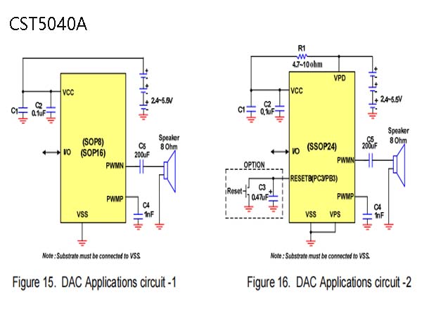
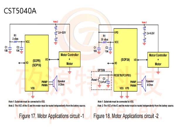
CST5040A/5041S1 The Application Circuit:
DAC Selected by option
Motor application


 Business consulting

 13823761625
 Mail me