


TRSF4A0XXA/B General Descriptions:
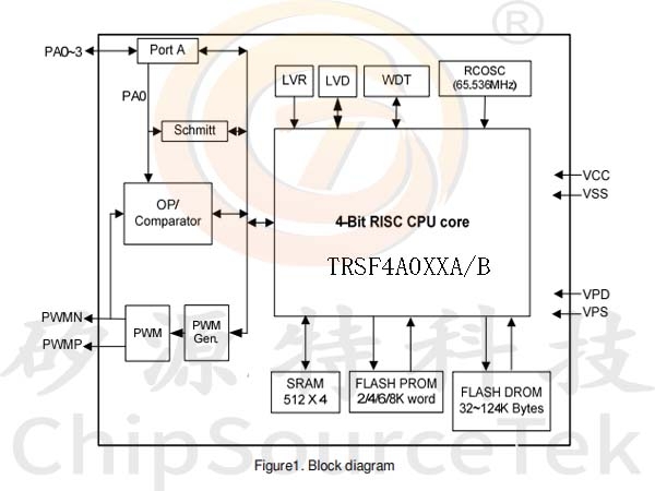
TRSF4A0XXA/B series are 4bit micro-controller which could play 4 channel melody or 4 channel ADPCM with PWM direct drive circuit. PWM resolution is 12 bits. They includes a low cost, high performance CMOS micro-processor. The clock frequency of this up is typically 13.1072 (±3%) MHz. This chip operates over a wide voltage range of 1.8V~5.5V. It contains program ROM and data ROM inside. The maximum program ROM is 8K word and data ROM size is 32K ~ 124K byte depending on PROM density. The maximum working SRAM is ( 512+2 ) nibbles. It provides with total 4 software programmable I/O Ports.
TRSF4A0XXA/B Features:
*Operating voltage: 1.8V to 5.5V
*Internal HROSC: 65.536 MHz, LRCOSC 32K Hz
-MCU Operation frequency: 13.1072 MHz
*Memory Size
-Flash Program Memory capacity: 2KX12, 4KX12, 6KX12 or 8KX12 bits selected by option.
-Flash Data ROM capacity: 32Kx8 ~ 124KX8 bits depending on PROM density.
-SRAM size: 512X4 bits
-User register: 2X4 bits
*Wakeup function for power-down mode
-HALT mode wakeup source: Port A, PWM and RTC wakeup can wake-up from HALT mode to NORMAL mode and executing wake-up sub-routine program.
*4 input/output pins: Port A can be defined as input or output port bit by bit.
*Three reset condition
-Low voltage reset (LVR = 1.7V)
-Power on reset
-Watch dog timer overflow
*One internal interrupt sources
-PWM interrupt
*WDT
-Watch dog timer, can enabled/disabled by option
-WDT period is 0.23 sec (Clock source by LRCOSC = 32.000K Hz ± 50%).
*Audio output
-Support 8/10/12 bits PWM
*Support option set for pull down resistor 1M/(50K or 220K), low voltage reset…etc.
*Oscillator fuse option ±3%, temperature & voltage compensation
*Support security option (1 bit) to protect user code.
*Low voltage detect ( LVD )
*12 sign x 8 unsigned multiplication
*Support indirect jump instruction JMPX, JMPPMA.
*Support direct call instruction CALLX, CALLPMA.
*Up to 8 level stacks for call sub-routing.
*TOUCH function: 4 I/O
*WKRTC
-Real-time clock in halt mode, can enabled/disabled by option
-wakeup period is 16/32/64/128 ms select by user code.
-Only operating on Halt mode.
( Clock source by LRCOSC = 32.000K Hz± 50%)
TRSF4A0XXA/B Block Diagram:

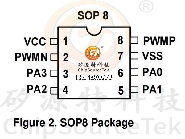
TRSF4A0XXA/B Package:
TRSF4A0XXA/B series provides SOP8

TRSF4A0XXA/B The Application Circuit
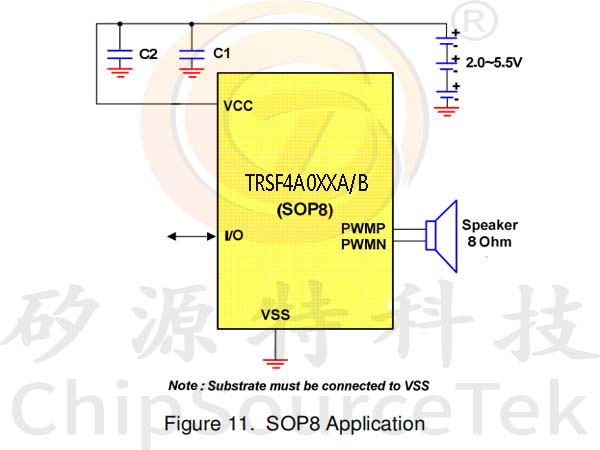
Notice:
1. C1 : 10 uF ~ 100 uF(depends on applications), C2:0.1 uF (high ESD protection).


 Business consulting

 13823761625
 Mail me