


PED2312A概述:
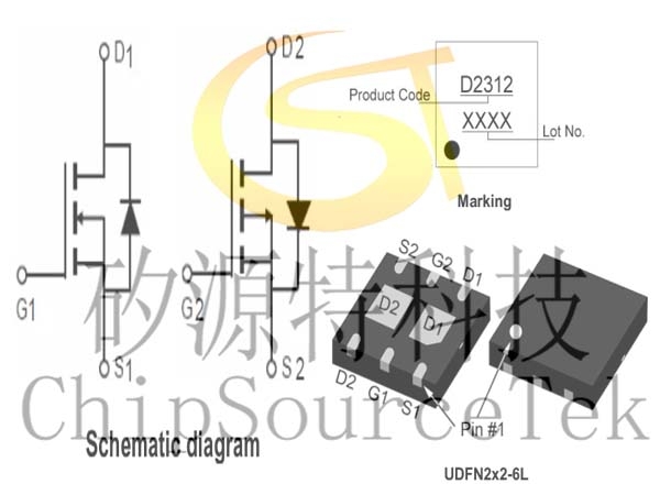
PED2312A是N-Channel:VDS=20V,ID=3.5A,RDS(ON)<45mΩ@VGS=4.5V,RDS(ON)<60mΩ@VGS=2.5V;P-Channel:VDS=-20V,ID=-3A,RDS(ON)<80mΩ@VGS=-4.5V,RDS(ON)<110mΩ@VGS=-2.5V的N+P双沟道MOSFET。PED2312A的丝印是D2312,PED2312A提供UDFN2x2-6L封装。
The PED2312A uses advanced trench technology to provide excellent RDS(ON) and low gate charge. It can be used in a wide variety of applications.
PED2312A特性:
N-Channel:
VDS = 20V, ID = 3.5A
RDS(ON) < 45mΩ@ VGS=4.5V
RDS(ON) < 60mΩ @VGS=2.5V
P-Channel
VDS = -20V, ID = -3A
RDS(ON) < 80mΩ @ VGS=-4.5V
RDS(ON) < 110mΩ @VGS=-2.5V
High Power and current handing capability
Lead free product is acquired
Surface Mount Package
PED2312A应用:
PWM applications
Power management
PED2312A典型应用及引脚:


 Business consulting

 13823761625
 Mail me