


P25D80SH Description/概述:
The P25D80SH is a serial interface Flash memory device designed for use in a wide variety of high-volume consumer based applications in which program code is shadowed from Flash memory into embedded or external RAM for execution. The flexible erase architecture of the device, with its page erase granularity it is ideal for data storage as well, eliminating the need for additional data storage devices.
The erase block sizes of the device have been optimized to meet the needs of today‘s code and data storage applications. By optimizing the size of the erase blocks, the memory space can be used much more efficiently. Because certain code modules and data storage segments must reside by themselves in their own erase regions, the wasted and unused memory space that occurs with large sectored and large block erase Flash memory devices can be greatly reduced. This increased memory space efficiency allows additional code routines and data storage segments to be added while still maintaining the same overall device density.
The device also contains an additional 3*512-byte security registers with OTP lock (One-Time Programmable), can be used for purposes such as unique device serialization, system-level Electronic Serial Number (ESN) storage, locked key storage, etc.
Specifically designed for use in many different systems, the device supports read, program, and erase operations with a wide supply voltage range of 2.3V to 3.6V. No separate voltage is required for programming and erasing.
P25D80SH是一种串行接口闪存设备,设计用于各种基于消费者的应用程序,程序代码从闪存隐藏到嵌入式或外部RAM执行。该设备灵活的擦除架构,其页面擦除粒度也是数据存储的理想选择,消除了对额外数据存储设备的需要。
该设备的擦除块大小已经被优化,以满足当今的代码和数据存储应用程序的需求。通过优化擦除块的大小,可以更有效地利用内存空间。由于某些代码模块和数据存储段必须自己驻留在它们自己的擦除区域中,因此,使用大分段和大块擦除闪存设备所产生的浪费和未使用的内存空间可以大大减少。这种提高的内存空间效率允许添加额外的代码例程和数据存储段,同时仍然保持相同的总体设备密度。
该设备还包含一个额外的3*512字节的安全寄存器与OTP锁(一次性可编程),可用于诸如唯一的设备序列化、系统级电子序列号(ESN)存储、锁定的密钥存储等目的。
专为许多不同的系统而设计,该设备支持读取、编程和擦除操作,电源电压范围为2.3V到3.6V。编程和擦除不需要单独的电压。
P25D80SH Overview:
General
Single 2.3V to 3.60V supply
Industrial Temperature Range -40C to 85C
Serial Peripheral Interface (SPI) Compatible: Mode 0 and Mode 3
Single, Dual SPI
- Standard SPI: SCLK,CS#,SI,SO,WP#,HOLD#
- Dual SPI: SCLK,CS#,IO0,IO1,WP#, HOLD#
Flexible Architecture for Code and Data Storage
- Uniform 256-byte Page Program
- Uniform 256-byte Page Erase
- Uniform 4K-byte Sector Erase
- Uniform 32K/64K-byte Block Erase
- Full Chip Erase
Hardware Controlled Locking of Protected Sectors by WP Pin
One Time Programmable (OTP) Security Register
- 3*512-Byte Security Registers With OTP Lock
128 bit unique ID for each device
Fast Program and Erase Speed
- 1.5ms Single/Dual page(s) program time
- 16ms Page erase time
- 16ms 4K-byte sector erase time
- 16ms 32K/64K-byte block erase time
JEDEC Standard Manufacturer and Device ID Read Methodology
Ultra Low Power Consumption
- 0.5uA Deep Power Down current
- 10.0uA Standby current
- 2.5mA Active Read current at 33MHz
- 3.0mA Active Program or Erase current
High Reliability
- 100,000 Program / Erase Cycles
- 10-year Data Retention
Industry Standard Green Package Options
- 8-pin SOP (150mil/208mil)
- 8-pin TSSOP
- KGD for SiP
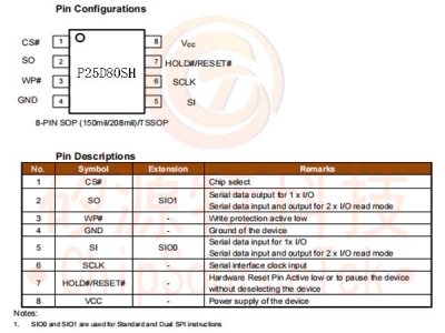
P25D80SH Pin Definition/引脚定义:

P25D80SH Block Diagram/结构框图:

P25D80SH Ordering Information:


 Business consulting

 13823761625
 Mail me