


Reducing Second Harmonic Distortion through Symmetric PCB Layout
Time:2023-06-08
Views:893
Differential circuits driven by differential signals do not generate even harmonics. In this article, we will discuss the necessity of using a symmetrical PCB layout to reduce second harmonic distortion. Even slight deviations from the symmetrical layout can increase the amplitude of the second harmonic by several decibels.
We will also discuss that it is signal path symmetry rather than component symmetry that actually determines the even distortion performance of the design.
Basic Techniques for Attenuating Second Harmonic
Driving symmetric structures through differential signals is usually a fundamental technique for suppressing second harmonic generation. Let‘s see how this technology works.
Suppose that our nonlinear circuit is memoryless (that is, the output at any time only depends on the input at the same time). We can approximate the nonlinear input output characteristics using the following equation:
Vout (t)= α 1vin (t)+ α 2vin2 (t)+ α 3vin3 (t)+ α 4vin4 (t)+ Vout (t)= α 1vin (t)+ α 2vin2 (t)+ α 3vin3 (t)+ α 4vin4 (t)+
Where vin (t) vin (t) and vout (t) vout (t) are the circuit input and output signals, respectively.
In this equation, the coefficient α one α 1 specifies the linear gain of the circuit, α two α 2 represents second harmonic distortion. To analyze the second harmonic, we can ignore the higher-order distortion coefficient( α 3, α 4,?) ( α 3, α 4,?) Obtain the following simplified equation:
Vout (t)= α 1vin (t)+ α 2vin2 (t) vout (t)= α 1vin (t)+ α 2vin2 (t)
If we use two copies of the circuit, one excited by input vin (t) vin (t) and the other excited by? Vin (t)? Under the excitation of vin (t), we will obtain the following outputs:
Vout,+(t)= α 1vin (t)+ α 2vin2 (t) vout,+(t)= α 1vin (t)+ α 2vin2 (t)
Vout,? (t)= α 1 (? Vin (t))+ α 2 (? Vin (t)) 2=? α 1vin (t)+ α 2vin2 (t) vout,? (t)= α 1 (? Vin (t))+ α 2 (? Vin (t)) 2=? α 1vin (t)+ α 2vin2 (t)
Subtracting these two outputs, we have:
Vout,+(t)? Vout,? (t) =2 α 1vin (t) out,+(t)? Vout,? (t) =2 α 1vin (t)
Although each circuit generates second harmonics, differential output can ideally suppress distortion components. This is a very important characteristic of differential operation and explains why differential circuits driven by differential signals do not generate even harmonics.
In fact, differential circuits may not be able to completely suppress even harmonics. However, compared to odd harmonics, even harmonics in differential structures can usually be ignored.
Example: Differential ADC interface can reduce second harmonic
The following figure shows an example application where two single ended signal paths are used to create a differential interface to ADS5500, a 14-bit, 125-MSPS analog-to-digital converter of TI.
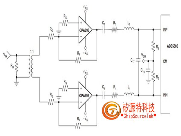


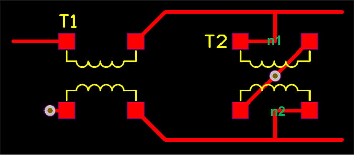
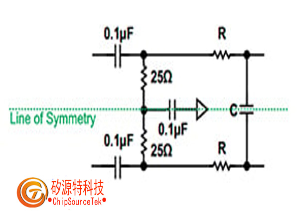
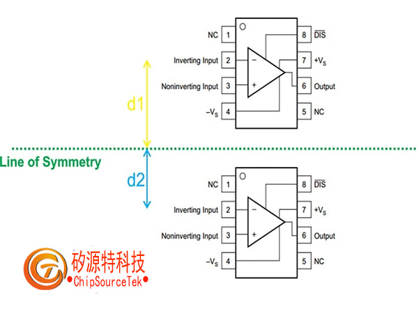
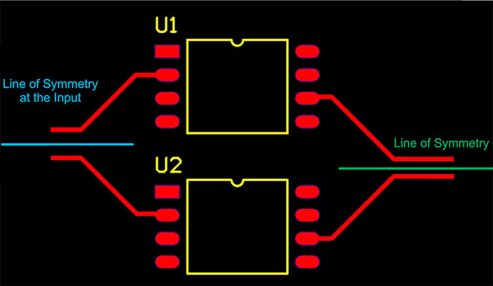
Figure 1, provided by TI.
The transformer converts a single ended input into a differential signal. After passing through the transformer, the two signal paths are identical.
It is worth mentioning that in practice, the transformer output is not an ideal differential signal - there may be phase and/or amplitude imbalance between the two outputs. These imbalances will increase second harmonic distortion. It can be seen that the amplitude of the second harmonic is more severely affected by phase imbalance than by amplitude imbalance.
Layout symmetry is the second harmonic suppression
In addition to using the same components in two signal paths, we also need to use a symmetrical PCB layout to minimize second harmonic generation. Asymmetric layout will prevent us from fully utilizing the linearity of active analog modules in the signal chain, such as ADCs and operational amplifiers.
For example, consider the ADC interface shown below.
Figure 3. Dual Balun topology for single ended to differential conversion.
For applications with SNR as the key parameter, this is a common circuit topology. Compared to using only a single balun structure, a dual balun configuration can reduce phase and amplitude imbalance between differential outputs. The AD9266 (Analog Devices‘ 16 bit 1.8 V ADC) data sheet recommends using a dual balanced unbalanced transformer structure to achieve frequencies greater than approximately 10 MHz.
Careful attention should be paid to the layout of this level to minimize second harmonic distortion.
Example layout of double balun structure
The two possible layouts of the double balun structure are shown in Figures 4 and 5.
Figure 4 is not an ideal layout because the routing from T1 to T2 is different for the upper and lower signal paths (i.e., x1 and x2 are different).
Another issue with this layout is the asymmetry of the two grounding pads of T2.
Figure 4. Asymmetric layout of dual balun configuration.
Figure 5 shows another layout of the circuit. In this case, the wiring connecting T1 and T2 runs to the midpoint (with an upper path of n1 and a lower path of n2), and then connects to the corresponding pads of T2. This makes the two paths the same. In addition, please note that the symmetrical wiring is used for the two grounding pads of T2.
Figure 5. Symmetrical layout.
Although these adjustments may seem subtle, they can have a significant impact on the distortion performance of the design. Compared with the layout shown in Figure 4, the symmetrical layout in Figure 5 can reduce the second harmonic amplitude by about 5dB.
Component symmetry and signal path symmetry
To obtain a symmetrical layout, sometimes we can start by placing components according to symmetrical lines. For example, the resistors and capacitors in Figure 2 above can be placed as shown in Figure 6.
Figure 6
For components at both ends such as resistors and capacitors, the placement of symmetrical components should lead to a symmetrical layout.
However, asymmetric packets are not in this situation. For example, consider an operational amplifier packaged in SOIC-8. As shown in Figure 7, placing two packages relative to a symmetrical line does not create a symmetrical layout. In this example, compared to the inverted input of the lower operational amplifier, the inverted input of the upper operational amplifier is further away from the symmetry line. In other words, d1>d2.
Figure 7
In these cases, we must consider different symmetry lines along the signal flow path to maintain signal symmetry.
Consider the following figure:
Figure 8
The following figure shows how changing the symmetry line allows us to maintain the symmetry of the signal path running to the inverting input and output of the operational amplifier.
|
Disclaimer: This article is transferred from other platforms and does not represent the views and positions of this site. If there is any infringement or objection, please contact us to delete it. thank you! |


 Business consulting

 13823761625
 Mail me