


Technical control is good, and all the knowledge about OLED technology is here
Time:2023-07-10
Views:765
OLED mainstream production technology
Steam plating technology
Firstly, it is important to understand the evaporation plating technology, which starts with the structure of OLEDs. As shown in the following figure, a typical structure is to make a layer of luminescent material several tens of nanometers thick on ITO glass. The ITO transparent electrode and metal electrode are used as the anode and cathode electrodes of the device to apply voltage. Under a certain voltage drive, electrons and holes are injected from the cathode and anode into the electron and hole transport layers, respectively. The electrons and holes migrate through the electron and hole transport layers to the luminescent layer, and meet and composite in the luminescent layer, The formation of excitons excites luminescent molecules, which undergo radiation relaxation and emit visible light. The radiated light can be observed from the ITO side, and the metal electrode film also acts as a reflective layer.
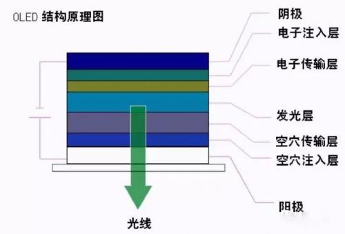
OLED structural schematic diagram
Of course, when it comes to the entire panel, the structure is also much more complex, including the need for isolation columns and insulation layers between sub pixels. AMOLED also has TFT backplane, which controls the switching of each pixel.
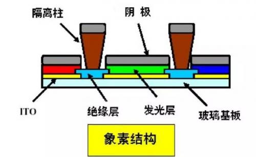
Schematic diagram of OLED pixel structure
Simply put, evaporation plating is the process of using current heating, electron beam bombardment heating, and laser heating in vacuum to evaporate the evaporated material into atoms or molecules, which then move in a straight line with a larger free path and collide with the substrate surface to condense, forming a thin film.
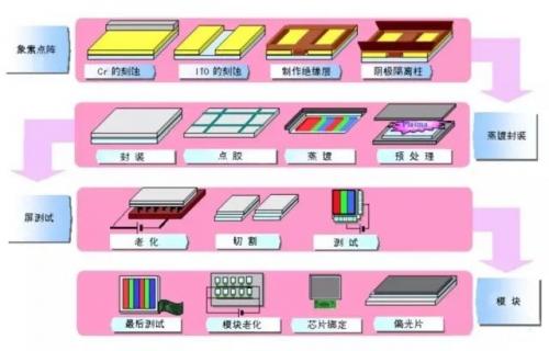
Typical Process Flow of PMOLED
(Note: PMOLED also belongs to OLED, but its structure is simpler than AMOLED and there is no TFT.)
Printing Technology
Each pixel "light bulb" on an OLED screen can not only be steamed on, but also be printed. For example, using an inkjet printer, it sprays ink onto paper to present a document or image. Printing display is a process that uses printing to produce an organic material film layer for displays. After achieving printing display, different panels can be printed. If OLED material is sprayed, it is an OLED panel; What is sprayed is quantum dot material, which is the quantum dot display panel. Printing OLED, in simple terms, refers to the precise deposition of polymer luminescent material solutions of different colors into the isolation column slots of ITO glass substrates through multiple printing heads on inkjet printing equipment. After the solvent evaporates, a thin layer of about 100 nanometers in thickness is formed, forming luminescent pixels.
Why is printing display technology the next generation display revolution? The vacuum evaporation plating process is limited by equipment and technology, making it difficult to produce large-sized fine metal masks, resulting in its inability to be applied to the manufacturing of large-sized panels. During the evaporation process, organic material gases deposit indiscriminately on the glass substrate, resulting in low material utilization. Perhaps due to the absence of vacuum evaporation chambers, precision metal masks, and color filters, Panasonic demonstrated a self-developed "printing" process at the 2013 CES exhibition, which, according to themselves, was the world‘s largest 4K OLED TV (56 inches) at that time.
What are the advantages of printing OLEDs that are sufficient to challenge relatively mature evaporation plating technology? Firstly, the cost is low. In the use of raw materials for OLED panels, printing OLED saves 90% compared to evaporation plating technology; Printing OLED technology can effectively improve the lifespan of finished products; The process of inkjet printing is easier to adapt to the cutting needs of large substrates than the evaporation process, which is more conducive to the trend of high generation line processing of large-sized substrates.
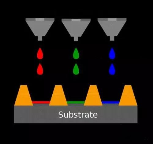
Schematic diagram of printing OLED implementation technology
According to industry insiders, the biggest bottleneck of printing OLEDs lies in controlling the differences between each tiny printing point (reducing the differences between pixels), as well as developing equipment for printing extremely small sub pixel units (improving equipment accuracy). The former is a key bottleneck in the entire printing and display industry, while the latter is mainly a problem for small and medium-sized display products. Alternatively, for printing OLEDs, ink stability is not the ultimate issue, but the equipment accuracy and stability are the real tests. This problem can only be truly solved from an engineering perspective after establishing a demonstration production line.
China Huaxing Optoelectronics, in collaboration with multiple key printing and display units in China, jointly established the first "Printing and Display Technology and Material Technology Innovation Alliance" in China, established a public technology service platform for printing and flexible displays, and used Guangdong Juhua Printing and Display Technology Co., Ltd. as the platform operating entity.
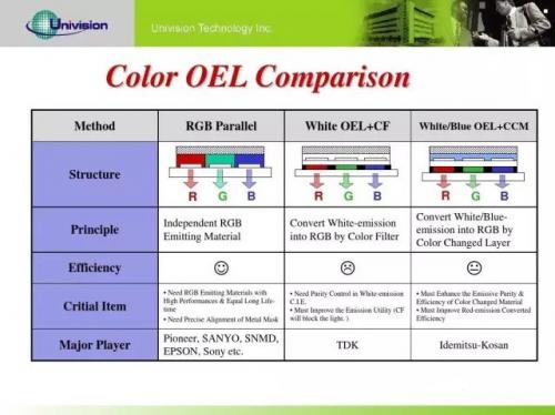
Three Implementation Schemes for OLED Screen Colors
The high-end and atmospheric "evaporation plating" method mentioned above is mainly applied to typical OLED screens arranged in RGB three colors. Many OLED TV products from Samsung are based on this method of evaporation plating, and the results are very good. The three primary colors are very pure, but the cost is very high. The technology used for this type of evaporation is called FMM, a fine metal mask, which covers a mask to distinguish pixels during evaporation. Therefore, alignment issues and the mask material itself become technical difficulties.
In fact, in order to control costs, OLED televisions are not just one of the above. There is a type of blue light+color conversion layer: this scheme only requires the evaporation of blue light OLED components, which are transformed into RGB three colors through the conversion layer. This type of technology is limited by the difficulty of developing color converters and has not been widely adopted.
Another type of OLED TV is white light with three types of color filters, which are similar in principle to LCD panels. With white as the backlight and color filters added, the cost is significantly lower. LG has used this solution to produce OLED TVs, and white light OLED with color filters was once considered a further low-cost solution for OLED. However, with the addition of filters, the transparency and color purity are all more problematic, so the brightness, contrast, color, and energy-saving performance are theoretically inferior to RGB OLEDs.
Research and Development Process and Technical Difficulties of AMOLED Flat Panel Display
The development of AMOLED technology mainly involves two aspects: TFT backplane and OLED devices. The choice of Technology roadmap has not been unified internationally at present, and there are many technical solutions under development.
The performance of light-emitting devices (OLEDs) determines the color expressiveness, power consumption and other qualities of AMOLED displays. Therefore, the development of OLED device technology is of great significance to the improvement of product competitiveness. There are two key points in the preparation technology of OLED devices. One is to develop high mobility transmission materials and high-efficiency, long-life luminescent materials, and the other is to develop new device structures to improve device performance. Therefore, developing new organic materials, designing new device structures, and improving vacuum evaporation technology will be the focus of research.
At present, the channel layer semiconductor materials in TFT backplanes mainly include amorphous silicon (a-Si) and microcrystalline silicon( μ- Si), Low-temperature polycrystalline silicon (LTPS), monocrystalline silicon, organics and oxides, etc. Due to OLED being a current driven device, a stable current is required to control the luminescent characteristics. In order to achieve sufficient brightness, AMOLED requires the channel material of TFT to have a high mobility to provide a high current density. Therefore, the amorphous silicon TFT commonly used in TFT-LCD is difficult to meet the requirements due to its low mobility. In addition, unlike TFT-LCD, AMOLED requires TFT to be turned on for a long time, and the threshold voltage drift problem of amorphous silicon TFT also makes it difficult to apply in AMOLED. From the perspective of State of the art, LTPS TFT, oxide TFT and other technologies are more promising, but there are also many difficulties.
At present, the most mature TFT backplane technology applied in AMOLED is Low-temperature polycrystalline silicon (LTPS) technology. The most important process difficulty in LTPS technology is the preparation of polycrystalline silicon channel layers. In the process flow, firstly, PECVD and other methods are used to deposit a layer of amorphous silicon on the glass substrate without alkali ions, and then laser or non laser methods are used to make the amorphous silicon film absorb energy, and atoms are rearranged to form a polysilicon structure, thus reducing defects and obtaining higher Electron mobility.
As far as LTPS crystallization technology is concerned, laser crystallization technology, especially Excimer laser annealing (ELA) technology, has been relatively mature in small-scale applications, and the world‘s mass produced AMOLED products have basically used ELA technology. The difficulty of ELA technology lies in the consistency of TFTs. The differences in TFT characteristics between pixels lead to uneven luminescence intensity of OLEDs, which in turn leads to the inability to guarantee panel yield. Therefore, improving the consistency of TFTs prepared by ELA technology has always been a focus of research and development by various units at home and abroad. In addition, ELA technology also has significant problems in mass production of large-sized substrates.
On the other hand, non laser crystallization technology has significant advantages in achieving mass production of large-sized substrates and reducing costs, as well as in terms of TFT uniformity. However, non laser crystallization technology also faces technical challenges at this stage. Among them, metal induced crystallization (MIC) technology is difficult to solve defects and lifespan issues due to leakage current caused by metal pollution; Solid phase crystallization (SPC) technology has significant comprehensive advantages in the preparation of large-sized AMOLED, but its carrier mobility is relatively low compared to laser crystallization technology, and further improvement is still needed in mass production technology.
AMOLED production process
The production process of LTPS-AMOLED includes many cutting-edge technologies in the display panel industry, mainly divided into three processes: backboard section, front board section, and module section. The backplane section process forms an LTPS (Low-temperature polycrystalline silicon) drive circuit through film forming, exposure, and etching overlay of films of different shapes and materials, which provides lighting signals and stable power input for light-emitting devices. The technical difficulties lie in the precision of the micron level process and the extremely high uniformity requirements for electrical indicators.
The coating process involves using coating equipment to physically or chemically deposit the required material onto a glass substrate (2);
The exposure process uses optical irradiation to transfer the patterns on the mask to the coated substrate (3, 4, 5) through photoresist printing;
The etching process is the use of chemical or physical methods to etch the film below the pattern on the substrate that is not covered by photoresist, and finally wash off the photoresist on the covering film, leaving a film layer (7, 8) with the desired pattern.
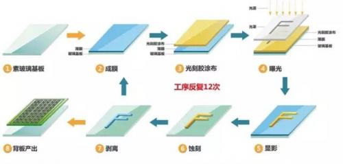
Process Flow Diagram of Drive Backboard
The front panel process uses high-precision metal mask (FMM) to evaporate organic light-emitting materials, cathodes and other materials on the backplane, combine them with the drive circuit to form light-emitting devices, and then package them in an oxygen free environment for protection. The alignment accuracy of evaporation plating and the airtightness of packaging are both challenges for the front panel process.
High precision optical mask (FMM): It is mainly made of materials with extremely low thermal deformation coefficients and is the key to defining pixel precision. After production, the FMM is accurately positioned on the metal frame by a mesh tensioning machine and sent to the evaporation and plating section (2);
The evaporation machine evaporates organic materials onto the defined area of the LTPS substrate through FMM under ultra-high vacuum (3);
After the evaporation coating is completed, the LTPS substrate is sent to the packaging section, and in a vacuum environment, it is bonded to the protective board using efficient glass adhesive that can block water vapor. The selection of glass adhesive and its application in the manufacturing process will directly affect the lifespan of OLEDs (5, 6).
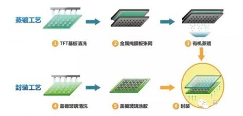
Process flow diagram of organic coating section
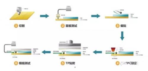
The module segment process cuts the packaged panel into actual product sizes, followed by various processes such as polarizer attachment, control circuit and chip bonding, aging testing, and product packaging, ultimately presenting the product in the hands of the customer.
Cutting: Cut the packaged AMOLED substrate into a panel (1);
Panel testing: Conduct panel illumination check (2);
Partial pasting: Attach the AMOLED panel to the polarizing plate (3);
IC+FPC binding: Link the driver IC and flexible printed circuit board (FPC) to the AMOLED panel (4);
TP attachment: Attach the AMOLED panel to the reinforced cover lenses containing touch sensors (5);
Module testing: aging test and lighting check of the module (6).
Process flow diagram of module section
|
Disclaimer: This article is transferred from other platforms and does not represent the views and positions of this site. If there is any infringement or objection, please contact us to delete it. thank you! |


 Business consulting

 13823761625
 Mail me