


Key Points for Low EMI Design of Class D Power Amplifier Chips
Time:2023-10-31
Views:515
Summary of key points
1 PVDD decoupling capacitor
10nF, 0603 package 2.2nF, 0603 package
PVDD pins are paired with decoupling capacitors, which should be placed on the same layer of PCB as the audio power amplifier chip as much as possible and as close to the power amplifier chip as possible.
1uF, 0603 package
Reasonably match the capacitance of ceramic capacitors, and try to keep it below 1 Ω within 100kHz~0.6GHz
(The basic impact range of Class D noise interference is within 300MHz), high switching frequencies (>768kHz) are usually recommended as 1uF+10nF (adjusted according to actual situation), and low switching frequencies are generally recommended as 4.7uF/10uF+100nF (adjusted according to actual situation)

1.1 Principle analysis of PVDD decoupling capacitor
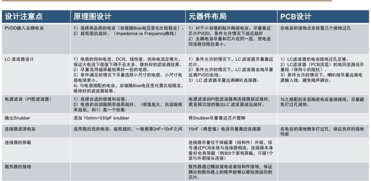
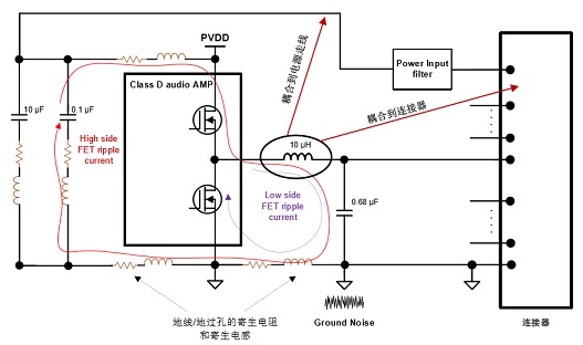
Source analysis of ground noise: Due to the parasitic inductance/resistance flowing through the switch ripple current, there is a voltage deviation between the reference ground and the power amplifier ground. Ground noise can be transmitted to the speaker line (or other wiring) through the audio amplifier, affecting the transmission/radiation test results.
Source analysis of power supply noise: Switching ripple current cannot be completely suppressed inside the small loop (red loop) through decoupling capacitors, resulting in ripple voltage on the Power Supply.
Layout precautions: Decoupling capacitors should be placed on the same layer as much as possible, as close as possible to the chip. The output current circuit of the LC filter should be as short as possible, the copper sheet should be laid as complete as possible, and the grounding vias of each capacitor should be sufficient to ensure the minimum return path impedance. The EMI of the decoupling capacitor placed on the same layer and close to the chip is reduced by~12dB compared to the scheme placed on the back (Bottom layer) between 75MHz and 100MHz
2. Output LC filter key indicators
• The three most critical indicators of inductance applied in Class D Amplifier (related to audio indicators):
• Maximum output current (in unsaturated conditions)
Sensitivity vs current curve (whether the sensitivity is stable after increasing the current)
• DC resistance
2. The most critical factors for EMI application in Class D Amplifiers are:
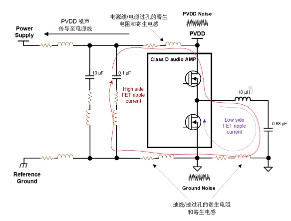
• Magnetic shielding performance. Try to choose an inductor with good magnetic shielding effect. Inductors with poor magnetic leakage are prone to interference with surrounding circuits, especially horn wires, power input wiring, or nearby connectors. The EMI interference frequency band caused by magnetic leakage of inductance is mainly concentrated in 30MHz
•Inductance size. The smaller the inductance size, the smaller the parasitic capacitance formed by the surrounding circuit, and the smaller the interference caused by the electric field. Usually affects the high-frequency section (>30MHz).
•Inductance value. Try to ensure a constant sensing value within the working current range and do not decrease too much.
Capacitance value. The capacitance value generally tends to decrease with the increase of working voltage. The higher the bias voltage, the more the capacitance value decreases. Pay attention to leaving sufficient margin when selecting capacitors.
2.1 PCB design considerations for outputting LC filters
1 LC filter should be as close to the chip as possible, the closer the better.
2 LC filters should be routed as far away from PVDD as possible. Due to the significant near-field interference of inductors, switching noise can be coupled to the wiring or components around the inductors. Keeping PVDD away from the inductor can improve the conductivity test results.
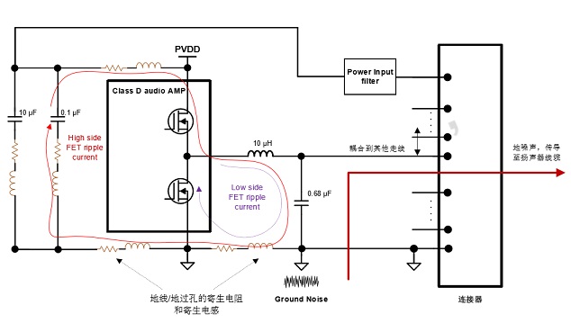
Try to keep the LC filter away from the connector as much as possible. Due to the significant near-field interference of inductance, switching noise can be coupled to connectors or cables, resulting in EMI interference.
A good connector shielding can avoid near-field interference from inductance.
Place sufficient grounding vias around the GND pad of the LC filter to ensure a sufficiently low noise return impedance.
Try to arrange a ground plane or ground wire on the PCB layer where the audio amplifier chip is located, so as to avoid through holes and obtain the lowest ground return impedance.
7. The speaker wiring can be routed in the inner or bottom layers to avoid coupling the switch noise on the speaker wiring to other wiring (such as coupling to the PVDD wiring).
Source analysis of ground noise: Due to the parasitic inductance/resistance flowing through the switch ripple current, there is a voltage deviation between the reference ground and the power amplifier ground. Ground noise can be transmitted to the speaker line (or other wiring) through the audio amplifier, affecting the transmission/radiation test results.
Layout precautions: The speaker wiring should be shielded on the inner layer as much as possible or avoided from other wiring on the back. The closer the LC filter is to the audio amplifier device, the better. Try to have as many grounding vias as possible for LC filters. Try to lay the ground on the same layer as the power amplifier chip to ensure the minimum grounding impedance.
2.3 Output LC Filter EMI Noise Link Analysis Part 2- Electric Field Radiation dV/dT
Analysis of the impact of electric field noise on the switching nodes and inductors of the power amplifier: Electric field noise usually comes from the switching nodes and inductors of the power amplifier, coupled to the cables of the PVDD wiring or connectors. The frequency band usually affected is above 30MHz.
Layout precautions: The LC filter should be as close to the chip as possible to reduce the electromagnetic radiation impact area of the power amplifier switch node; Try to use small-sized inductors; Keep the LC filter away from the PVDD wiring and connectors; Shielding the connector is the most effective method.

2.4 Output LC Filter EMI Noise Link Analysis Part 3- Magnetic Field Radiation dI/dT
Analysis of the impact of magnetic field noise on inductors: Inductors in this province are a relatively strong source of magnetic field noise, coupled to PVDD wiring or connectors of cables. The frequency band usually affected is within 30MHz.
Layout precautions: During the LC filter design process, try to choose inductors with low magnetic leakage (usually, integrated metal alloy inductors can improve EMI by more than 7dB in the frequency range of 30MHz compared to open frame ferrite inductors); Keep the LC filter away from the PVDD wiring and connectors;
A good magnetic shielding inductance has a difference of 7dB to 17dB in the impact between 2MHz and 30MHz compared to a poor magnetic shielding inductance.

3 power supply PI type filter
L1, C40, C41, and C42 form an EMI filter on the power line
Generally, the sensitivity value of L1 should be between 0.68uH and 4.7uH
The higher the self resonant frequency (SRF) of the inductor, the better (preferably greater than 70MHz). The smaller the inductance value, the higher the self resonant frequency generally. The magnitude of the inductance and the self resonant frequency are a trade-off in system design.
4. Precautions for horn connector design
4.1 Place a~10nF chip ceramic capacitor near the pin of each connector, as close as possible to the connector. This method generally has an improvement of~6dB around 75MHz.
4.2The specific capacitance value of this capacitor can be adjusted based on the actual EMI test results.
4.3 Place enough ground vias to ensure that these capacitors have a good grounding path.
4.4 The switching nodes of the audio amplifier and the inductance generate strong dV/dT noise. If the LC filter is placed too close to the connector, the electric field energy will be directly coupled to the connector or speaker/power line, thereby directly affecting the conduction and radiation test results. Effective shielding of the connector (with the shield grounded) can have a relatively good effect, usually improving by~5dB between 100MHz and 200MHz. When the LC filter itself is relatively close to the connector, the improvement is more significant, usually exceeding 15dB for the FM and DAB frequency bands (174MHz~239MHz).
5 Radiator PCB grounding shield
Generally, the heat sink has a large area and is susceptible to noise coupling on the PCB board. It is best to ensure that the radiator and amplifier have a nearby grounding point. All noise coupled to the heat sink can flow back to the audio amplifier in the shortest path, thereby reducing radiation.
In some cases, the grounded and ungrounded heat sink can cause a 9dB EMI index difference even in the frequency range of 100MHz to 200MHz.
|
Disclaimer: This article is transferred from other platforms and does not represent the views and positions of this site. If there is any infringement or objection, please contact us to delete it. thank you! |


 Business consulting

 13823761625
 Mail me