


What exactly is the driving capability of IO
Time:2024-01-23
Views:266
It is common to hear that the driving capability of an MCU I/O is xxmA, so what exactly is driving capability? If the driving capacity of a certain IO is 5mA, can it not output a current exceeding 5mA? Why are there differences in the driving capabilities of IO?
 At this point, the driving ability refers to the ability of the I/O pin to output logic 0 normally under the condition that the maximum input current is less than or equal to. The same principle applies, the greater the current flowing through N-MOS, the greater the voltage drop generated by N-MOS, and the greater the voltage at the I/O port. When the voltage reaches the highest voltage Vol of logic 0, the current at this time represents the driving ability.
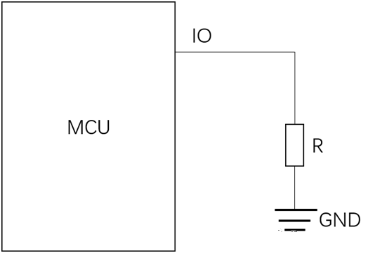 An external resistor is connected to GND on the IO pin of the MCU. As long as this resistor is not too small, the voltage of the IO pin remains basically unchanged, with only a slight decrease. When the resistance is small and the current is high, the voltage will significantly decrease.
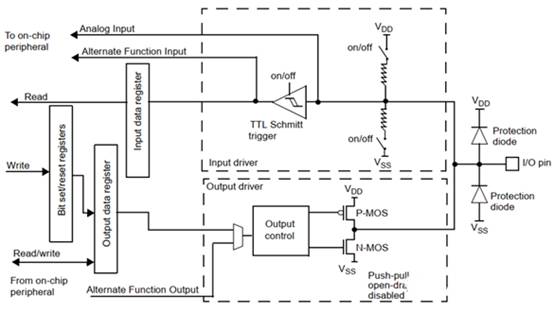
To answer the above questions, it is necessary to first understand the internal I/O structure of the MCU,
(This image is sourced from the STM32F103 reference manual)
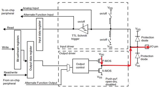
When outputting high-level 1, the internal VDD of the I/O flows through the PMOS to the I/O pin, as shown by the red arrow in the following figure,
At this point, the driving ability refers to the ability of the I/O pin to output logic 1 normally when the output current is less than or equal to the maximum output current.
The source (S) of the P-MOS transistor is connected to the VDD. When the MCU outputs 1, the P-MOS transistor conducts, and the current flows from the source (S) to the drain (D). The current and VDS (source drain voltage) flowing through the P-MOS transistor will vary depending on the size of the external load on the I/O pin. The larger the output current, the larger the VDS, and the smaller the I/O voltage. When the voltage drops to Voh, the output current indicates the driving capability.
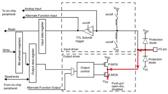
When the output is low level 0, the I/O pin flows through N-MOS to the internal VSS of the I/O, as shown by the red arrow in the following figure
After reading the above clearly, the answers to the three questions at the beginning of the article are also available,
1) I/O drive capability refers to the maximum amount of current that can be output and absorbed while simultaneously satisfying Voh (minimum voltage value when output pin is logic 1) and Vol (maximum voltage value when output pin is logic 0). The values of Voh and Vol can be found in the chip data manual.
2) If the driving capacity of a certain I/O is 5mA, it does not mean that it cannot output a current exceeding 5mA. However, when the output current exceeds 5mA, its output voltage will decrease and the voltage will be less than Voh.
3) The difference in I/O driver capability comes from the characteristics of MOSFETs themselves. To achieve high current capability, the volume of MOSFETs needs to be larger, the required area of the chip will be larger, and the cost will naturally be higher. So usually, MCU only has a portion of I/O with high driving capacity, and not every I/O is made with high driving capacity.
Having said so much, we can actually explain it with the following simple circuit,
Interested parties can actually test it, but be careful not to set the current too high and burn out the IO.
|
Disclaimer: This article is transferred from other platforms and does not represent the views and positions of this site. If there is any infringement or objection, please contact us to delete it. thank you! |


 Business consulting

 13823761625
 Mail me