


Discussion on the architecture and design considerations of charge pumps
Time:2024-01-30
Views:254
Switching power supplies can be divided into two categories: inductive switching power supplies and capacitive switching power supplies. The key components that play a role in energy storage in power sources are inductors and capacitors. Capacitor switching power supply, also known as charge pump, can achieve boost, buck, and reverse phase in the power supply.
.gif)

1. Understanding of charge pump architecture
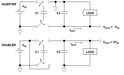
The core of the charge pump is to change the series parallel relationship between capacitors through a switch based on their energy storage characteristics, thereby changing the output voltage. The process of charge pump energy storage and transfer can be understood from the following figure. Core device switches and flying capacitors. The charge pump is no longer limited to low-power (tens, hundreds of mA) schemes, but there are already high-power schemes such as the ADI LTC7821 scheme.
Figure 1
2. Classification of charge pumps
Charge pumps can be divided into non stabilized charge pumps and stabilized charge pumps.
A. From the architecture in Figure 1, we can see that the output voltage is doubled and inverted by the input voltage, and the output voltage will vary with the input voltage. This structure can achieve voltage requirements of double voltage, half voltage, reverse phase, and fractional ratio, but the specific requirements depend on the internal topology of the chip.
B. Stable output voltage is usually required in power supply, so internal architecture control requires closed-loop.
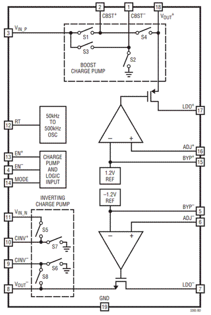
Figure 2- The interior of ADI LTC3265 appears to be a charge pump architecture+LDO architecture, achieving stable positive and negative power output.
Figure 3- The internal architecture of ADI ADP3605 appears to be a charge pump architecture that adjusts stable output by adding output feedback to regulate the conduction resistance of the loop control switch.
Overall, the charge pump with non stable voltage architecture has higher efficiency than these two charge pumps with stable output voltage.
Figure 3
3. Design considerations
Overall, the peripheral circuit of the charge pump is relatively simple, small in size, high in efficiency, with core components such as switches and flying capacitors. To achieve optimal power performance, comprehensive considerations must be taken from device selection to PCB layout and wiring. For example, whether the switch device is built-in or external, the corresponding switch speed and switch loss; The type, capacitance value, loss, size, and other conventional parameters of capacitors.
Flying capacitor: Due to the need to reverse the polarity of the capacitor during switching, ceramic capacitors are preferred. X5R or X7R ceramic capacitors maintain good performance at -40 ° C-85 ° C.
Input and output capacitors: In order to improve efficiency while reducing output noise and ripple, it is recommended to use ceramic capacitors with low ESR. To increase the transient required charge capacity, tantalum capacitors and electrolytic capacitors can be connected in parallel. Ripple voltage is often closely related to switching frequency, output current, capacitance value, and ESR and requires comprehensive consideration.
Switching MOSFET: The switching frequency of the charge pump is usually in the range of tens of KHz to a few MHz. Some high-power charge pumps are equipped with external switching transistors, and in addition to the driving of the transistors, switching losses and conduction losses must also be considered.
4. Application scenarios
Charge pumps can be used in scenarios of high-power fast charging of mobile devices
Charge pumps can be used in scenarios with low current requirements of less than 200mA inside portable devices
Charge pump can be used for driving LCD and LED
In our commonly used RS232 level conversion and some power supply, hot swappable chips, etc., we can also see the use of charge pumps as MOSFET gate drivers
In scenarios that require negative voltage and small current, a charge pump is also a very good choice
Overall, the charge pump circuit is simple, with certain advantages in terms of volume and efficiency, and its usage scenarios are increasing.
|
Disclaimer: This article is transferred from other platforms and does not represent the views and positions of this site. If there is any infringement or objection, please contact us to delete it. thank you! |


 Business consulting

 13823761625
 Mail me