


IP6833 Brief Introduction:
IP6833 is a highly integrated, efficient, and WPC Qi compliant wireless charging receiver chip. The chip integrates a fully synchronous rectification circuit, power output circuit, reverse protection circuit with an efficiency of over 95%, extremely low heat loss, and a good application experience. The internally integrated dynamic rectification voltage control effectively improves the transient response and system efficiency of the chip.
IP6833 adopts a QFN28 (4mm * 4mm) ultra-small package, combined with a simplified peripheral application circuit, which greatly saves PCB board area and can be easily integrated into compact products. At the same time, the chip has undergone overall impedance optimization, greatly reducing the heating of the chip itself and improving the charging performance of small space product applications.
IP6833 has a built-in low-power MCU, which can be upgraded online through firmware updates, providing a flexible design approach for developing complete terminal device solutions. Equipped with a built-in 12 bit ADC, it can accurately calculate the battery level. Supports switching between wireless and wired charging paths.
IP6833 has a built-in 1.6A voltage regulating LDO, providing a maximum charging current of 800mA for linear charging, and can flexibly configure the maximum charging current. Built in IC temperature and input voltage intelligent adjustment charging current function.
IP6833 Features:
High Integration Single Chip Wireless Charging Reception Scheme
-Integrated MCU
-Complies with WPC Qi BPP control standards
-Built in high-efficiency synchronous rectification circuit, with an efficiency of over 95%
Dynamic rectification voltage control
-Enhance transient performance
-Optimize load efficiency
Built in 1.6A voltage regulating LDO
Built in 800mA Charger
Supports switching between wired and wireless charging paths
Minimalist peripheral circuit, simple application, low cost
Supporting complete protection for over temperature, over voltage, and over current with 16V overvoltage protection
Ultra low power consumption, standby<3uA
QFN28 package (4mm * 4mm)
IP6833 Application:
Wireless charging receiving device compatible with WPC Qi standard
Wearable products such as smartwatches and smart wristbands
Health and medical equipment such as hearing aids
Various low-power handheld devices
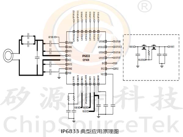
IP6833 Typical application schematic diagram:
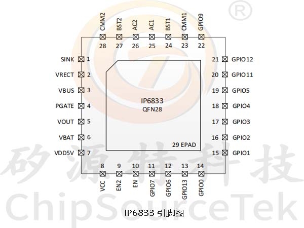
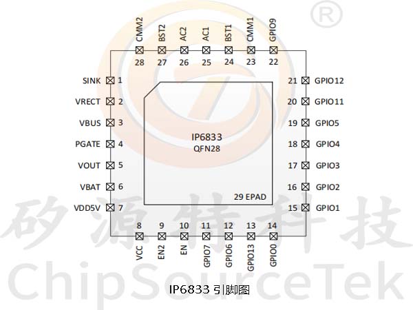
IP6833 Pin Definition:
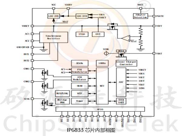
IP6833 Internal block diagram of the chip:
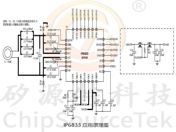
IP6833 Application schematic diagram:


 Business consulting

 13823761625
 Mail me