


ZB25VQ32D Description/概述:
The ZB25VQ32D of non-volatile flash memory device supports the standard Serial Peripheral Interface (SPI). Traditional SPI single bit serial input and output (Single I/O or SIO) is supported as well as optional two bit (Dual I/O or DIO) and four bit (quad I/O or QIO) serial protocols. This multiple width interface is called SPI Multi-I/O or MIO.
The ZB25VQ32D support the standard Serial Peripheral Interface (SPI), Dual/Quad I/O SPI as well as 2-clocks instruction cycle Quad Peripheral Interface (QPI): Serial Clock, Chip Select, Serial Data I/O0 (DI), I/O1 (DO), I/O2 (WP#), and I/O3 (HOLD#/RESET#). SPI clock frequencies of up to 133MHz are supported allowing equivalent clock rates of 266MHz (133MHz x 2) for Dual I/O and 532MHz (133MHz x 4) for Quad I/O when using the Fast Read Dual/Quad I/O and QPI instructions. These transfer rates can outperform standard Asynchronous 8 and 16-bit Parallel Flash memories. The Continuous Read Mode allows for efficient memory access with as few as 8-clocks of instruction-overhead to read a 24-bit address, allowing true XIP (execute in place) operation.
A Hold pin, Write Protect pin and programmable write protection, with top or bottom array control, provide further control flexibility. Additionally, the device supports JEDEC standard manufacturer and device ID and SFDP Register, a 128-bit Unique Serial Number and three 1024-Byte Security Registers.The ZB25VQ32D provides an ideal storage solution for systems with limited space, signal connections, and power. These memories‘ flexibility and performance is better than ordinary serial flash devices. They are ideal for code shadowing to RAM, executing code directly (XIP), and storing reprogrammable data.
ZB25VQ32D非易失性闪存设备支持标准串行外设接口(SPI)支持传统的SPI单位串行输入和输出(单I/O或SIO)以及可选的两个位(双I/O或DIO)和四位(四I/O或QIO)串行协议。这种多宽度接口称为SPI多I/O或MIO。
ZB25VQ32D支持标准串行外设接口(SPI)、双/四路I/O SPI以及2块指令周期四外设接口(QPI):串行时钟,芯片选择,串行数据I/O 0(DI),I/O1(DO)、I/O2(WP#)和I/O3(保持#/RESET#)。支持高达133MHz的SPI时钟频率允许双输入/输出的等效时钟频率为266MHz(133MHz x 2),四输入/输出为532MHz(133MHz x 4)当使用快速读取双/四路I/O和QPI指令时。这些传输速率可以优于标准传输速率异步8位和16位并行闪存。连续读取模式允许高效存储只需8个时钟的指令开销即可读取24位地址,从而实现真正的XIP(在场所)操作。
保持引脚、写入保护引脚和可编程写入保护,具有顶部或底部阵列控制,提供进一步的控制灵活性。此外,该设备支持JEDEC标准制造商和设备ID以及SFDP寄存器、一个128位唯一序列号和三个1024字节安全寄存器。ZB25VQ32D为具有有限空间、信号连接等的系统提供了理想的存储解决方案,和权力。这些存储器的灵活性和性能都优于普通的串行闪存设备。他们是非常适合将代码隐藏到RAM、直接执行代码(XIP)和存储可编程数据。
ZB25VQ32D Features/特性:
Power Supply Voltage
- Single 2.3V-3.6V supply
32M bit Serial Flash
- 32 M-bit/4M-Byte/16,384 pages
- 256 Bytes per programmable page
- Uniform 4K-Byte Sectors, 32K/64K-Byte Blocks
New Family of SPI Flash Memories
- Standard SPI: CLK, CS#, DI, DO, WP#, HOLD#/RESET#
- Dual SPI: CLK, CS#, DI, DO, WP#, HOLD# /RESET#
- Quad SPI: CLK, CS#, IO0, IO1, IO2, IO3
- QPI: CLK, CS#, IO0, IO1, IO2, IO3
- Software & Hardware Reset
- Auto-increment Read capability
Temperature Ranges
- Industrial (-40°C to 85°C)
- Industrial (-40°C to 105°C)
Low power consumption
- 1 μA typical standby current, HFM =0
- 15 μA typical standby current, HFM =1
- 1 μA typical power down current
Efficient “Continuous Read” and QPI Mode
- Continuous Read with 8/16/32/64-Byte Wrap
- As few as 8 clocks to address memory
- Quad Peripheral Interface (QPI) reduces instruction overhead
Flexible Architecture with 4KB sectors
- Sector Erase (4K-Byte)
- Block Erase (32K/64K-Byte)
- Page Program up to 256 Bytes
- More than 100K erase/program cycles
- More than 20-year data retention
Advanced Security Feature
- Software and Hardware Write-Protect
- Power Supply Lock-Down and OTP protection
- Top/Bottom, Complement array protection
- 128-Bit Unique ID for each device
- Serial Flash Discoverable Parameters (SFDP) Register
- 3X1024-Byte Security Registers with OTP locks
- Volatile & Non-volatile Status Register Bits
High performance program/erase speed
- Page program time: 500us typical
- Sector erase time: 45ms typical
- Block erase time: 250ms typical
- Chip erase time: 12s typical
Package Options
- SOP8 - 150mil / 208mil
- DFN8 (2*3*0.55mm)
- DFN8 (4*3*0.55mm)
- TFBGA24
- All Pb-free packages are RoHS compliant
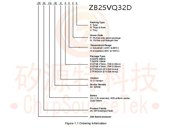
ZB25VQ32D Ordering Information:

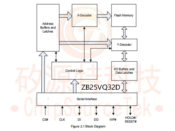
ZB25VQ32D Block Diagram:
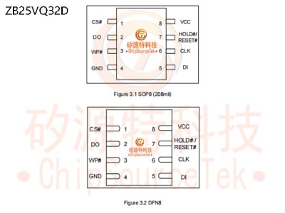
ZB25VQ32D Connection Diagrams:


 发送邮件
发送邮件 商务QQ客服
 13823761625

