


XT25F08B-S General Description:
The XT25F08B-S (8M-bit) Serial flash supports the standard Serial Peripheral Interface (SPI), and supports the Dual/Quad SPI: Serial Clock, Chip Select, Serial Data I/O0 (SI), I/O1 (SO), I/O2 (WP#), and I/O3 (HOLD#). The Dual I/O data is transferred with speed of 216Mbits/s and the Quad I/O & Quad output data is transferred wit speed of 432Mbits/s.
XT25F08B-S Features:
8M -bit Serial Flash
1024K-byte
256 bytes per programmable page
Support SFDP & Unique ID
Standard, Dual,Quad SPI
Standard SPI: SCLK, CS#, SI, SO, WP#, HOLD#
Dual SPI: SCLK, CS#, IO0, IO1, WP#, HOLD#
Quad SPI: SCLK, CS#, IO0, IO1, IO2, IO3
FlexibleArchitecture
Sector of 4K-byte
Block of 32/64k-byte
Advanced security Features
4*256-Byte Security Registers WithOTP Lock
Software/HardwareWrite Protection
Write protect all/portion of memory via software
Enable/Disable protection withWP# Pin
Top or Bottom, Sector or Block selection
Package Options
See 1.1 Available Ordering OPN
All Pb-free packages are compliant RoHS, Halogen-Free and REACH.
Known Good Die “KGD”version
Temperature Range & Moisture Sensitivity Level
Industrial Level Temperature. (-40℃ to +85℃), MSL3
Low Power Consumption
15uA typical standby current
0.06uA typical deep power down current
Single Power SupplyVoltage: Full voltage range:
2.7~3.6V
2.7~3.6V
Minimum 100,000 Program/Erase Cycle
High Speed Clock Frequency
108MHz for fast read with 30PF load
Dual I/O Data transfer up to 216Mbits/s
Quad I/O Data transfer up to 432Mbits/s
Program/EraseSpeed
Page Program time: 0.4mstypical
Sector Erase time: 70mstypical
Block Erase time: 0.15/0.25stypical
Chip Erase time: 2.5stypical
XT25F08B-S Available Ordering OPN:
|
OPN
|
Package Type
|
Package Carrier
|
|
XT25F08BSOIGU-S
|
SOP8 150mil
|
Tube
|
|
XT25F08BSOIGT-S
|
SOP8 150mil
|
Tape & Reel
|
|
XT25F08BSSIGU-S
|
SOP8 208mil
|
Tube
|
|
XT25F08BSSIGT-S
|
SOP8 208mil
|
Tape & Reel
|
|
XT25F08BDFIGT-S
|
DFN8 2x3x0.55 mm
|
Tape & Reel
|
XT25F08B-S Connection Diagram:
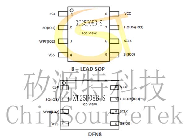
XT25F08B-S Pin Description:
|
Pin Name
|
I/O
|
Description
|
|
CS#
|
I
|
Chip SelectInput
|
|
SO (IO1)
|
I/O
|
Data Output (Data Input Output 1) |
|
WP# (IO2)
|
I/O
|
Write Protect Input (Data Input Output 2) |
|
VSS
|
|
Ground
|
|
SI (IO0)
|
I/O
|
Data Input (Data Input Output 0) |
|
SCLK
|
I
|
Serial Clock Input
|
|
HOLD#
|
I/O
|
Hold Input (Data Input Output 3) |
|
VCC
|
|
Power Supply
|
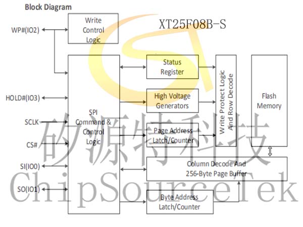
XT25F08B-S Block Diagram:


 发送邮件
发送邮件 商务QQ客服
 13823761625

