


XT25F16B General Description:
The XT25F16B (16M-bit) Serial flash supports the standard Serial Peripheral Interface (SPI), and supports the Dual/Quad SPI: Serial Clock, Chip Select, Serial Data I/O0 (SI), I/O1 (SO), I/O2 (WP#), and I/O3 (HOLD#). The Dual I/O data is transferred with speed of 240Mbits/s and the Quad I/O & Quad output data is transferred with speed of 480 Mbits/s.
XT25F16B Features:
16M -bit Serial Flash
2048K-byte
256 bytes per programmable page
Standard, Dual, Quad SPI
Standard SPI: SCLK, CS#, SI, SO, WP#, HOLD#
Dual SPI: SCLK, CS#, IO0, IO1, WP#, HOLD#
Quad SPI: SCLK, CS#, IO0, IO1, IO2, IO3
Flexible Architecture
Sector of 4K-byte
Block of 32/64k-byte
Advanced security Features
3*256-Byte Security Registers With OTP Lock
Software/Hardware Write Protection
Write protect all/portion of memory via software
Enable/Disable protection with WP# Pin
Top or Bottom, Sector or Block selection
Package Options
See 1.1 Available Ordering OPN
All Pb-free packages are compliant RoHS, Halogen-Free and REACH.
Temperature Range & Moisture Sensitivity Level
Industrial Level Temperature. (-40℃ to +85℃), MSL3
Industrial Plus Level Temperature. (-40℃ to +105℃), MSL1
Low Power Consumption
20mA maximum active current
5uA maximum power down current
Single Power Supply Voltage: Full voltage range:
2.7~3.6V
Minimum 100,000 Program/Erase Cycle
High Speed Clock Frequency
120MHzfor fast read with 30PF load
Dual I/O Data transfer up to 240Mbits/s
Quad I/O Data transfer up to 480Mbits/s
Program/Erase Speed
Page Program time: 0.4ms typical
Sector Erase time: 100mstypical
Block Erase time: 0.15/0.25stypical
Chip Erase time: 6s typical
XT25F16B Available Ordering OPN:
|
OPN
|
Package Type |
Package Carrier |
|
XT25F16BSOI/HGU
|
SO8 150mil
|
Tube
|
|
XT25F16BSOI/HGT
|
SO8 150mil
|
Tape & Reel
|
|
XT25F16BSSI/HGU
|
SO8 208mil
|
Tube
|
|
XT25F16BSSI/HGT
|
SO8 208mil
|
Tape & Reel
|
|
XT25F16BSSI/HGA
|
S08 208mil
|
Tray
|
|
XT25F16BTSI/HGU
|
TSSOP8 173mil
|
Tube
|
|
XT25F16BTSI/HGT
|
TSSOP8 173mil
|
Tape & Reel
|
|
XT25F16BDFI/HGT
|
DFN8 2x3x0.55 mm
|
Tape & Reel
|
|
XT25F16BDXI/HGT
|
DFN8 4x3x0.55 mm
|
Tape & Reel
|
|
XT25F16BDSI/HGT
|
DNF8 4x4x0.55 mm |
Tape & Reel |
|
XT25F16BDTI/HGT
|
DFN8 2x3x0.40 mm |
Tape & Reel |
|
XT25F16BWOI/HGA
|
WSON 6*5 mm |
Tray |
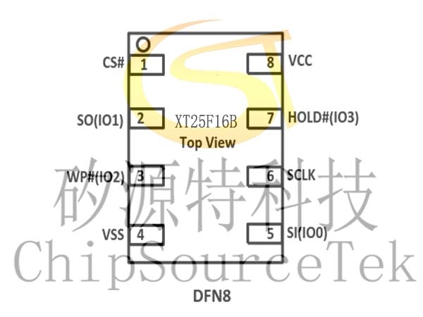
XT25F16B Connection Diagram:
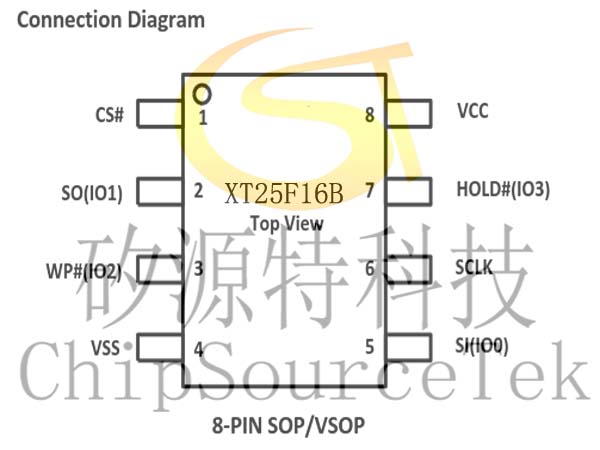

XT25F16B Pin Description:
|
Pin Name
|
I/O
|
Description
|
|
CS#
|
I
|
Chip Select Input
|
|
SO (IO1)
|
I/O
|
Data Output (Data Input Output 1) |
|
WP#(IO2)
|
I/O
|
Write Protect Input (Data Input Output 2) |
|
VSS
|
|
Ground
|
|
SI (IO0)
|
I/O
|
Data Input (Data Input Output 0) |
|
SCLK
|
I
|
Serial Clock Input
|
|
HOLD# (IO3)
|
I/O
|
Hold Input (Data Input Output 3) |
|
VCC
|
|
Power Supply
|
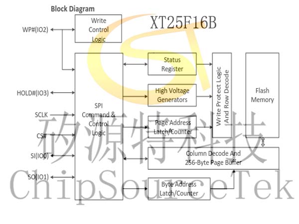
XT25F16B Block Diagram:


 发送邮件
发送邮件 商务QQ客服
 13823761625

